Interleaved conductor structure with offset traces

Active Publication Date: 2012-06-28
WESTERN DIGITAL TECH INC
0 Cites 10 Cited by

AI-Extracted Technical Summary

Problems solved by technology

Smaller slider structures generally require more compliant gimbals, hence the intrinsic stiffness of the conductor wires attached to the head slider can give rise to a significant undesired bias effect.
Because the conductor traces are positioned extremely close to, but electrically isolated from, the conductive stainless steel flexure structure which is in turn grounded to the load beam, and because of the relatively high ...

Benefits of technology

[0008]The present invention generally provides for an interleaved conductor structure for electrically connecting a read/write head in a hard disk drive. The disclosed interleaved condu...

Abstract

An interleaved conductor structure for electrically connecting the read/write electronics to a read/write head in a hard disk drive is provided. The interleaved conductor structure may allow for an increased characteristic-impedance range, greater interference shielding and a reduction of signal loss that is contributed by a lossy conductive substrate. The electrical traces may have different widths, be offset, or even wrap around each other at the via connections.

Application Domain

Record information storageInsulated cables +5

Technology Topic

Hard disc driveElectricity +4

Image

  • Interleaved conductor structure with offset traces
  • Interleaved conductor structure with offset traces
  • Interleaved conductor structure with offset traces

Examples

  • Experimental program(2)

Example

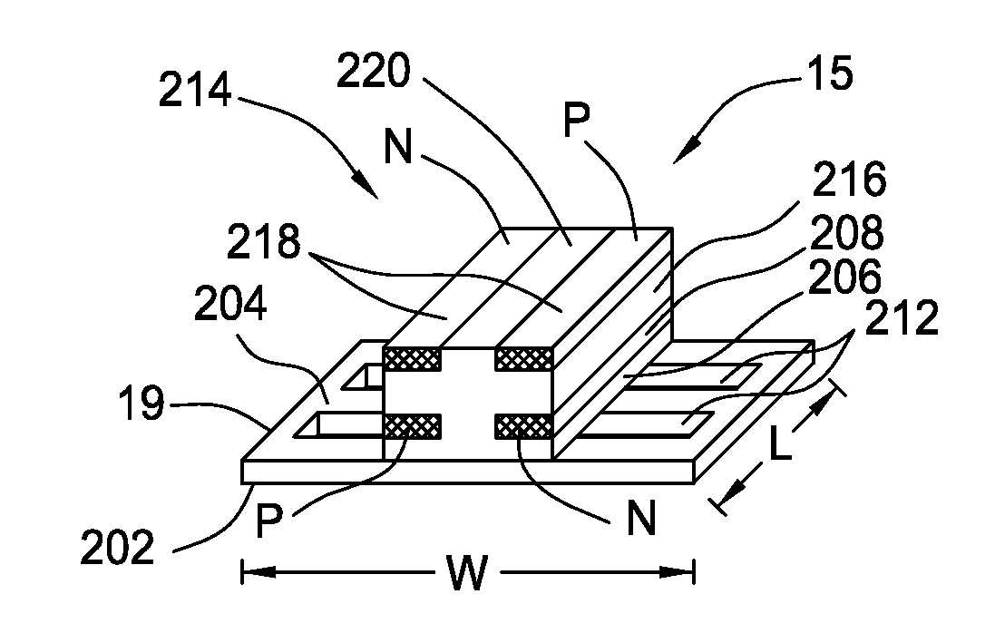
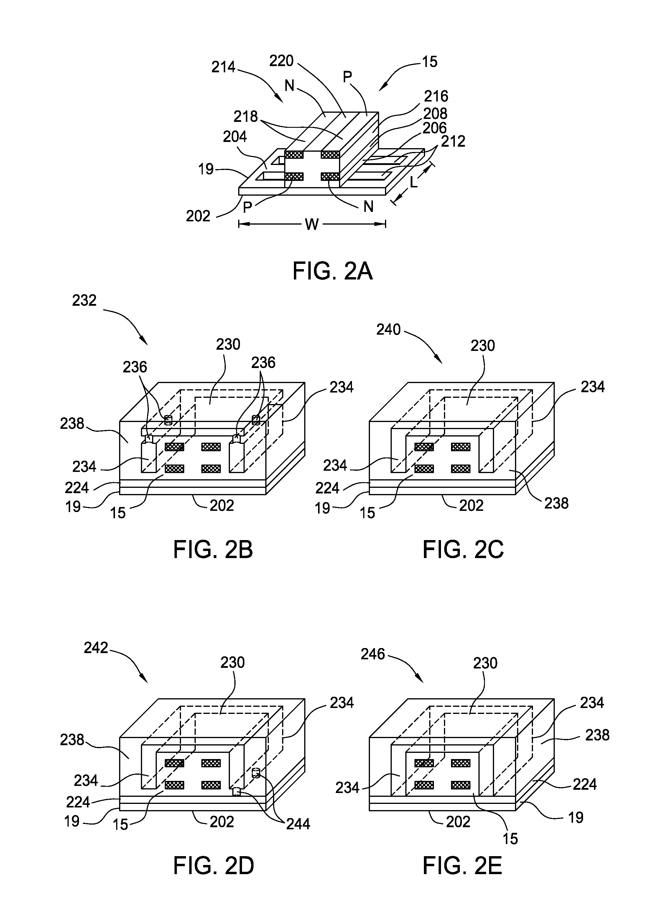
[0035]FIG. 2C depicts a cross sectional isometric view of a sixth embodiment of the interleaved conductor structure 240. The interleaved conductor structure 240 is substantially similar to the interleaved conductor structure 232 of FIG. 2B. However, in the interleaved conductor structure 240 the conductive sidewalls 234 extend completely to the top conductive shield layer 230, without the need for the plurality of vias 236. By extending the conductive sidewalls 234 to the top conductive shield layer 230, the electrical connection between the conductive sidewalls 234 and the top conductive shield layer 230 is improved, and a more continuous shield structure is formed.

Example

[0036]In FIG. 2D a cross sectional isometric view of a seventh embodiment of the interleaved conductor structure 242 is shown. The interleaved conductor structure 242 is substantially similar to the interleaved conductor structure 240 of FIG. 2C. However, in the interleaved conductor structure 242 a plurality of vias 244 electrically connects the conductive sidewalls 234 to the first conductive layer 224. In some embodiments, the first conductive layer 224 is omitted, and the vias 244 connect the conductive sidewalls 234 to the conductive underlayer 19. By electrically connecting the conductive sidewalls 234 (and the top conductive shield layer 230) to the underlying support, the shield structure is at the same electrical potential as the underlying support, thereby providing improved control of the characteristic impedance and improved shielding.
[0037]FIG. 2E depicts a cross sectional isometric view of an eighth embodiment of the interleaved conductor structure 246. The interleaved conductor structure 246 is substantially similar to the interleaved conductor structure 242 of FIG. 2D. However, in the interleaved conductor structure 246 of FIG. 2E the conductive sidewalls 234 extend to contact the first conductive layer 224, without the need for the plurality of vias 244. By extending the conductive sidewalls 234 to the first conductive layer 224, the electrical connection between the conductive sidewalls 234 and the first conductive layer 224 is improved, and a more continuous shield structure is formed. In some embodiments, the first conductive layer 224 is omitted, and the conductive sidewalls 234 extend to the conductive underlayer 19. In one embodiment, the interleaved conductor structure 246 provides a shield structure that completely surrounds the electrical connection assembly 15 similar to the shield in a coaxial cable.
[0038]FIG. 3A is a schematic isometric view of an interleaved conductor structure 300 according to one embodiment. The structure 300 includes a bottom conductive layer 302 and a first electrical insulation layer 304 formed thereover. The first electrical insulation layer 302 may be patterned to form slots into which a first plurality of electrical traces 306 are formed. In the embodiment shown in FIG. 3A, there are two electrical traces 306 with one being a positive phase trace (labeled P) and one being a negative phase trace (labeled N). An area 314 of electrical insulation remains between the traces 306. A second electrical insulation layer 308 is formed over the first plurality of electrical traces306. Similar to the first electrical insulation layer 304, the second electrical insulation layer 308 is patterned to form slots into which a second plurality of electrical traces 310 are formed. In the embodiment shown in FIG. 3A, there are two electrical traces 310 with one being a positive phase trace (labeled P) and one being a negative phase trace (labeled N). An area 316 of electrical insulation remains between the traces 310. A third electrical insulation layer 312 is formed over the second plurality of electrical traces 310.
[0039]The first plurality of electrical traces 306 have a first width B and the second plurality of electrical traces 310 have a second width A. The bottom or first plurality of electrical traces 306 are wider than the top or second plurality of electrical traces 310. The distance between adjacent traces of the first plurality of electrical traces 306 is substantially equal to the distance between adjacent traces of the second plurality of electrical traces 310 as shown by arrow C. The width of the traces 306, 310 is within about 30 percent to about 85 percent of each other. It is contemplated that the width of the traces 306, 310 may be within about 50 percent to about 75 percent of each other. In the embodiment shown in FIG. 3A, at least one edge of each trace of the second plurality of electrical traces 310 is vertically aligned with at least one edge of a trace of the first plurality of electrical traces 306 that is directly therebelow.
[0040]It can be quite difficult to produce traces of the exact same width on two different levels in which the edges are vertically aligned. Therefore, to increase the manufacturing tolerance, the second plurality of electrical traces 310 may simply be disposed over the first plurality of electrical traces 306 without regard to whether any edges are aligned. The second plurality of electrical traces 310 may be centered over the first plurality of electrical traces 306 rather than having at least one edge aligned. In the embodiment shown in FIG. 3A, the bottom or first plurality of electrical traces 306 has a greater width than the top or second plurality of electrical traces 310 so that the bottom or first plurality of electrical traces 306 may be used as a reference when forming the top or second plurality of electrical traces 310. It is contemplated that the top or second plurality of electrical traces 310 may be formed anywhere within the width of the first plurality of electrical traces 306. Even though the traces 306, 310 have different widths, there is no impedance dropoff. In particular, the impedance range for the structure 300 may be between about 10 ohm to about 40 ohm. While not shown, it is contemplated that the second plurality of electrical traces 310 may have a greater width than the first plurality of electrical traces 306.
[0041]It is contemplated that more than two layers of traces may be utilized. FIGS. 3B-3D are schematic isometric illustrations of three layer trace structures. In FIG. 3B, the interleaved conductor structure 320 has a third plurality of electrical traces 322 formed above the third electrical insulation layer 312. A fourth electrical insulation layer 324 is formed thereover. In the embodiment of FIG. 3B, the first plurality of electrical traces 306 has a width E that is greater than the width of both the second plurality of electrical traces 310 and the third plurality of electrical traces 322. However, the second plurality of electrical traces 310 and the third plurality of electrical traces 322 have substantially the same width as shown by arrows D. Additionally, in the embodiment shown in FIG. 3B, at least one edge of all of the traces 306, 310, 322 is vertically aligned and thus, are spaced apart by substantially the same distance as shown by arrow F. Similar to FIG. 3A, the bottom or first plurality of electrical traces 306 has a greater width than both the second plurality of electrical traces 310 and the third plurality of electrical traces 322 so that the first plurality of electrical traces 306 may be used as a reference when forming the second plurality of electrical traces 310 and the third plurality of electrical traces 322. It is contemplated that the second plurality of electrical traces 310 and the third plurality of electrical traces 322 may be formed anywhere within the width of the first plurality of electrical traces 306.
[0042]In the embodiment shown in FIG. 3C, interleaved conductor structure 330 has three separate trace levels. The second plurality of electrical traces 310 has a greater width than both the first plurality of electrical traces 306 and the third plurality of electrical traces 322. The first plurality of electrical traces 306 and the third plurality of electrical traces 322 have substantially the same diameter and at least one edge of each trace is vertically aligned with another trace. Similar to FIG. 3B, the second plurality of electrical traces 310 may be used as a reference when forming the third plurality of electrical traces 322. It is contemplated that the first plurality of electrical traces 306 and the third plurality of electrical traces 322 may be formed anywhere within the width of the second plurality of electrical traces 310.
[0043]In the embodiment shown in FIG. 3D, the interleaved conductor structure 340 has three separate trace levels. The third plurality of electrical traces 322 and the first plurality of electrical traces 306 have a greater width than the second plurality of electrical traces 310. The first plurality of electrical traces 306 and the third plurality of electrical traces 322 have substantially the same diameter and at least one edge of each trace is vertically aligned with another trace. Similar to FIG. 3B, the first plurality of electrical traces 306 may be used as a reference when forming the second plurality of electrical traces 310 and the third plurality of electrical traces 322. It is contemplated that the second plurality of electrical traces 310 may be formed anywhere within the width of the second plurality of electrical traces 310.
[0044]As shown in FIG. 3E, the interleaved conductor structure 350 may have a conductive overlayer 352 on top of an electrical insulation layer as has been described above. It is to be understood that each conductors structure discussed herein in each embodiment is contemplated to have one or more of a conductive overlayer 352, one or more apertures 212 formed through the conductive underlayer 19, vias 244, conductive sidewalls 234 and outer dielectric material 238 as described above. The conductive overlayer 352, the bottom conductive layer 302, the conductive sidewalls 234 each can individually function to shield the traces and to reduce the impedance.
[0045]As shown by FIGS. 3F and 3G, the spacing between the traces for may be different. The first plurality of electrical traces 306 have a spacing G that is less than the spacing for the second plurality of electrical traces 310 as shown by H in FIG. 3F. However, the second plurality of traces 310 are each disposed within the width of a corresponding trace of the first plurality of traces 306. In FIG. 3G, the second plurality of traces 310 are again spaced a greater distance as shown by J as compared to the first plurality of traces 306 as shown by I. However, one of the traces of the second plurality of electrical traces 310 has an edge that is vertically aligned with an edge of a corresponding trace of the first plurality of electrical traces 306. Another trace of the second plurality of electrical traces 310 is substantially centered over a corresponding trace of the first plurality of electrical traces 306. It is to be understood that while FIGS. 3F and 3G refer to embodiments where the first plurality of electrical traces 306 have a greater width than the second plurality of electrical traces 310, the spacing differences apply equally to the situation where the first plurality of electrical traces 306 have a smaller width than the second plurality of electrical traces 310.
[0046]FIGS. 4A and 4B are isometric views showing interleaved conductor structures 400, 430 according to various embodiments of the invention. In FIGS. 4A and 4B, the traces at the different levels are offset and have a serpentine appearance. FIGS. 4A and 4B show interleaved conductor structures 400, 430 having a bottom conductive layer 402, an electrical insulation layer 404 formed thereover, a first plurality of conductive traces 406 formed within a slot in the first electrical insulation layer 404, a second electrical insulation layer 408 formed over the first plurality of electrical traces 406, and a second plurality of electrical traces 410 formed within slots that are cut into the second electrical insulation layer 408. In each of FIGS. 4A and 4B, the second plurality of electrical traces 410 are offset from the first plurality of electrical traces 406.
[0047]Offsetting the second plurality of electrical traces 410 from the first plurality of electrical traces 406 increases the impedance range of the structures 400, 430 relative to structures in which the traces are not offset. More specifically, the offset provides a wider characteristic impedance range for the structures 400, 430. Offsetting the second plurality of electrical traces 410 from the first plurality of electrical traces 406 from center increases the impedance. The adjustability afforded by offsetting the traces allows for more control over the impedance in the final design of the structure 400, 430. In FIGS. 4A and 4B, the offset is periodic such that each trace pair has a different impedance level (Z=sqrt(L/C)) increasing the inductance (L), and decreasing the capacitance (C) between the second plurality of electrical traces 410 and the first plurality of electrical traces 406. Therefore, trace swapping between the second plurality of electrical traces 410 and the first plurality of electrical traces 406 is important to keep the desired impedance level. The impedance requirements in the final design of the hard drive could be altered by preamp/arm-electronics design specifications (e.g., to match the impedance), read-write head design specification (e.g., to match the impedance), scalability (e.g., different armature length between 3.5″ and 2.5″ drives), and the need for additional traces for the next generation drives (e.g., for the thermal fly-height control, thermal assisted writing, and thermal asperity detection). The periodic maximum trace length should be set to less than 1/10 of the wavelength of the maximum symbol transfer rate; whereas the periodicity does not have a significant effect on the impedance levels for the required frequency range (symbol transfer). Lower periodic trance lengths would cause ripples in the time-domain response.
[0048]In the embodiments shown in FIGS. 4A and 4B, the first plurality of electrical traces 406 each have the same width. Similarly, the second plurality of electrical traces 410 each have the same width. The width of the first plurality of electrical traces 406 is substantially equal to the width of the second plurality of electrical traces 410. The distance between adjacent traces in the first plurality of electrical traces 406 is substantially equal to the width of each of the second plurality of electrical traces 410. Similarly, the distance between adjacent traces in the second plurality of electrical traces 410 is substantially equal to the width of each of the first plurality of electrical traces 406. Thus, any cross-talk effects are balanced. Additionally, the traces are vertically aligned along the edges.
[0049]FIGS. 5A and 5B are schematic top view illustrations of trace layout patterns according to various embodiments of the invention. It is to be understood that the trace layout patterns shown in FIGS. 5A and 5B are applicable to the interleaved conductor structures discussed above. FIG. 5A shows a two level trace pattern. For the first plurality of electrical traces 500, the positive phase trace has two ends 502, 506 connected by a middle section 510. Similarly, the negative phase trace has two ends 504, 508 connected by a middle section 512. Over the first plurality of electrical traces 500, an insulating layer may be deposited over which the second plurality of electrical traces 501 is formed. The second plurality of conductive traces 501 includes a positive phase trace and a negative phase trace. The negative phase trace of the second plurality of electrical traces 501 is connected to the negative phase trace of the first plurality of electrical traces 500 at the ends 516, 520 to the ends 504, 508 of the negative phase trace of the first plurality of electrical traces 500. The ends 516, 520, 504, 508 are connected by vertical vias formed through the intervening layers. However, even though the negative phase trace of the second plurality of electrical traces 501 is connected to the negative phase trace of the first plurality of electrical traces 500, the middle section 530 of the negative phase trace of the second plurality of electrical traces 501 is vertically aligned with the middle section 510 of the positive trace of the first plurality of electrical traces 500. In order to vertically align the middle sections 530, 510, the negative phase trace of the second plurality of electrical traces 501 wraps around the end 518 of the positive phase trace of the second plurality of electrical traces 501 with a wrap around section 528 and the trace angles over by way of a slanted portion 532 to the middle section 530.
[0050]Similarly, the positive phase trace of the second plurality of electrical traces 501 is connected to the positive phase trace of the first plurality of electrical traces 500 at the ends 514, 518 to the ends 502, 506 of the positive phase trace of the first plurality of electrical traces 500. The ends 514, 518, 502, 506 are connected by vertical vias formed through the intervening layers. However, even though the positive phase trace of the second plurality of electrical traces 501 is connected to the positive phase trace of the first plurality of electrical traces 500, the middle section 522 of the positive phase trace of the second plurality of electrical traces 501 is vertically aligned with the middle section 512 of the negative phase trace of the first plurality of electrical traces 500. In order to vertically align the middle sections 522, 512, the positive phase trace of the second plurality of electrical traces 501 wraps around the end 516 of the negative phase trace of the second plurality of electrical traces 501 with a wrap around section 522 and the trace angles over by way of a slanted portion 526 to the middle section 522.
[0051]Thus, the negative phase trace of the second plurality of electrical traces 501 has one loop and one slanted portion. Similarly, the positive phase trace of the second plurality of electrical traces also has one loop and one slanted portion. Therefore, negative phase trace and the positive phase trace of the second plurality of electrical traces 501 have substantially the same length so that the impedance is balanced. By wrapping the ends of one trace around the end of a second trace that is at the same level, the end of one trace does not need to pass under or over the second trace. Of course, the second plurality of electrical traces 501 have a longer length than the first plurality of electrical traces 500. It is to be understood that the first plurality of electrical traces 500 and the second plurality of electrical traces 501 could be reversed such that the second plurality of electrical traces 501 are below the first plurality of electrical traces 500.
[0052]FIG. 5B shows a four level trace pattern. Similar to FIG. 5A, the first plurality of electrical traces 540 includes a positive phase trace having ends 541, 542 and a middle section 543 connecting the ends 541, 542. The first plurality of electrical traces 540 also includes a negative phase trace having ends 546, 547 as well as a middle section 545 connecting the ends 546, 547. Over the first plurality of electrical traces 540, an insulating layer may be deposited over which the second plurality of electrical traces 550 is formed. The second plurality of conductive traces 550 includes a positive phase trace and a negative phase trace. The negative phase trace of the second plurality of electrical traces 550 is connected to the negative phase trace of the first plurality of electrical traces 540 at the ends 553, 554 to the ends 546, 547 of the negative phase trace of the first plurality of electrical traces 550. The ends 546, 547, 553, 554 are connected by vertical vias formed through the intervening layers. However, even though the negative phase trace of the second plurality of electrical traces 550 is connected to the negative phase trace of the first plurality of electrical traces 540, the middle section 555 of the negative phase trace of the second plurality of electrical traces 550 is vertically aligned with the middle section 543 of the positive trace of the first plurality of electrical traces 540. In order to vertically align the middle sections 555, 543, the negative phase trace of the second plurality of electrical traces 550 wraps around the end 551 of the positive phase trace of the second plurality of electrical traces 550 with a wrap around section 558 and the trace angles over by way of a slanted portion 557 to the middle section 555.
[0053]Similarly, the positive phase trace of the second plurality of electrical traces 550 is connected to the positive phase trace of the first plurality of electrical traces 540 at the ends 551, 552 to the ends 541, 542 of the positive phase trace of the first plurality of electrical traces 540. The ends 541, 542, 551, 552 are connected by vertical vias formed through the intervening layers. However, even though the positive phase trace of the second plurality of electrical traces 550 is connected to the positive phase trace of the first plurality of electrical traces 540, the middle section 556 of the positive phase trace of the second plurality of electrical traces 550 is vertically aligned with the middle section 545 of the negative phase trace of the first plurality of electrical traces 540. In order to vertically align the middle sections 556, 545, the positive phase trace of the second plurality of electrical traces 550 wraps around the end 553 of the negative phase trace of the second plurality of electrical traces 550 with a wrap around section 559 and the trace angles over by way of a slanted portion 560 to the middle section 556.
[0054]Over the second plurality of electrical traces 550, another insulation layer may be deposited. Thereover, a third plurality of electrical traces 570 may be formed. The third plurality of electrical traces 570 includes a positive phase trace having ends 571, 572 connected by a middle section 573. The positive phase trace is vertically aligned with the positive phase trace of the first plurality of electrical traces 540 and connected thereto at the ends 571, 572, 541, 542 through vias formed through intervening layers. The positive phase trace is also connected to the ends 551, 552 of the positive phase trace of the second plurality of electrical traces 550. Similarly, the third plurality of electrical traces 570 includes a negative phase trace having ends 574, 575 connected by a middle section 576. The negative phase trace is vertically aligned with the negative phase trace of the first plurality of electrical traces 540 and connected thereto at the ends 574, 575, 547, 546 through vias formed through intervening layers. The negative phase race is also connected to the ends 557, 558 of the negative phase trace of the second plurality of electrical traces 550.
[0055]Over the third plurality of electrical traces 570, an insulating layer may be deposited over which the fourth plurality of electrical traces 580 is formed. The fourth plurality of conductive traces 580 includes a positive phase trace and a negative phase trace. The negative phase trace of the fourth plurality of electrical traces 580 is connected to the negative phase trace of the third plurality of electrical traces 570 at the ends 586, 590 to the ends 574, 575 of the negative phase trace of the third plurality of electrical traces 570. The ends 574, 575, 586, 590 are connected by vertical vias formed through the intervening layers. However, even though the negative phase trace of the fourth plurality of electrical traces 580 is connected to the negative phase trace of the third plurality of electrical traces 570, the middle section 588 of the negative phase trace of the fourth plurality of electrical traces 580 is vertically aligned with the middle section 573 of the positive trace of the third plurality of electrical traces 570. In order to vertically align the middle sections 588, 573, the negative phase trace of the fourth plurality of electrical traces 580 wraps around the end 585 of the positive phase trace of the fourth plurality of electrical traces 580 with a wrap around section 589 and the trace angles over by way of a slanted portion 587 to the middle section 588.
[0056]Similarly, the positive phase trace of the fourth plurality of electrical traces 580 is connected to the positive phase trace of the third plurality of electrical traces 570 at the ends 581, 585 to the ends 571, 572 of the positive phase trace of the third plurality of electrical traces 570. The ends 571, 572, 571, 585 are connected by vertical vias formed through the intervening layers. However, even though the positive phase trace of the fourth plurality of electrical traces 580 is connected to the positive phase trace of the third plurality of electrical traces 570, the middle section 583 of the positive phase trace of the fourth plurality of electrical traces 580 is vertically aligned with the middle section 576 of the negative phase trace of the third plurality of electrical traces 570. In order to vertically align the middle sections 583, 576, the positive phase trace of the fourth plurality of electrical traces 580 wraps around the end 586 of the negative phase trace of the fourth plurality of electrical traces 580 with a wrap around section 582 and the trace angles over by way of a slanted portion 585 to the middle section 583.
[0057]In FIG. 5B, the positive phase traces of both the first plurality of electrical traces 540 and the third plurality of electrical traces 570 are vertically aligned and have substantially the same length. Similarly, the negative phase traces of both the first plurality of electrical traces 540 and the third plurality of electrical traces 570 are vertically aligned and have substantially the same length. The positive phase traces of both the second plurality of electrical traces 550 and the fourth plurality of electrical traces 580 are vertically aligned and have substantially the same length. Similarly, the negative phase traces of both the second plurality of electrical traces 550 and the fourth plurality of electrical traces 580 are vertically aligned and have substantially the same length. Both the positive phase trace and the negative phase trace of the first plurality of electrical traces 540 have substantially the same length and thus, substantially the same impedance. Both the positive phase trace and the negative phase trace of the second plurality of electrical traces 550 have substantially the same length and thus, substantially the same impedance. Both the positive phase trace and the negative phase trace of the third plurality of electrical traces 570 have substantially the same length and thus, substantially the same impedance. Both the positive phase trace and the negative phase trace of the fourth plurality of electrical traces 580 have substantially the same length and thus, substantially the same impedance.
[0058]While the foregoing is directed to embodiments of the present invention, other and further embodiments of the invention may be devised without departing from the basic scope thereof, and the scope thereof is determined by the claims that follow.

PUM

no PUM

Description & Claims & Application Information

We can also present the details of the Description, Claims and Application information to help users get a comprehensive understanding of the technical details of the patent, such as background art, summary of invention, brief description of drawings, description of embodiments, and other original content. On the other hand, users can also determine the specific scope of protection of the technology through the list of claims; as well as understand the changes in the life cycle of the technology with the presentation of the patent timeline. Login to view more.

Similar technology patents

Printed circuit board and preparation method thereof

PendingCN111988927AReduce signal lossImprove signal transmission quality
Owner:SHENNAN CIRCUITS

Package structure and method of fabricating the same

ActiveUS20160135299A1shorten signal pathreduce signal loss
Owner:PHOENIX PIONEER TECH

Reducing High-Frequency Signal Loss in Substrates

ActiveUS20100164069A1reduce signal loss
Owner:TAIWAN SEMICON MFG CO LTD

Packaged antenna module and preparation method thereof

PendingCN112289766AReduce signal lossincrease flexibility
Owner:SJ SEMICON JIANGYIN CORP +1

State monitoring protection device

InactiveCN101752833AReduce signal lossImprove overall accuracy
Owner:上海瑞视仪表电子有限公司
Why Eureka
Try Eureka