

Bidirectional shockley diode with extended mesa
- Summary
- Abstract
- Description
- Claims
- Application Information
AI Technical Summary
Benefits of technology
Problems solved by technology
Method used
Image

Examples
Embodiment Construction
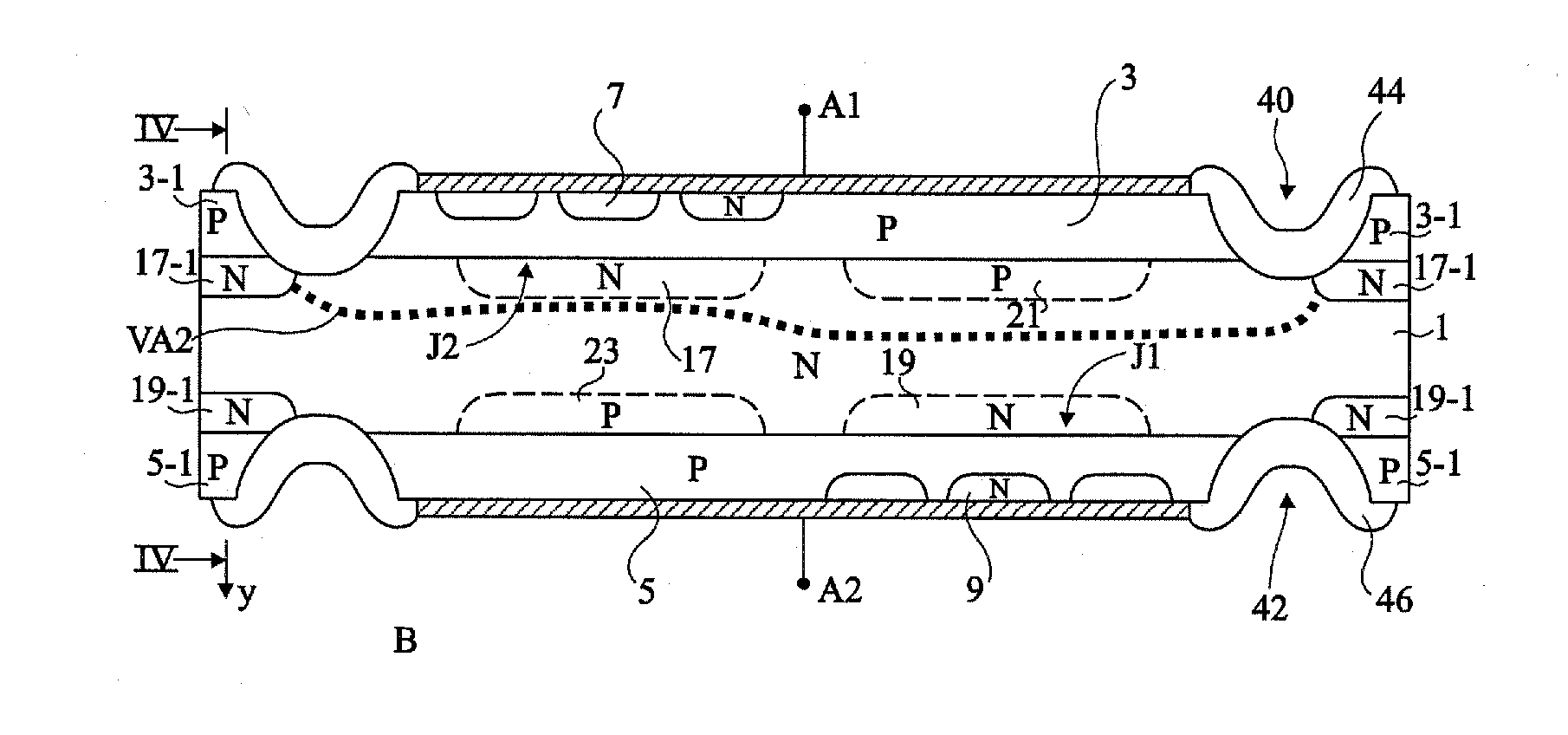
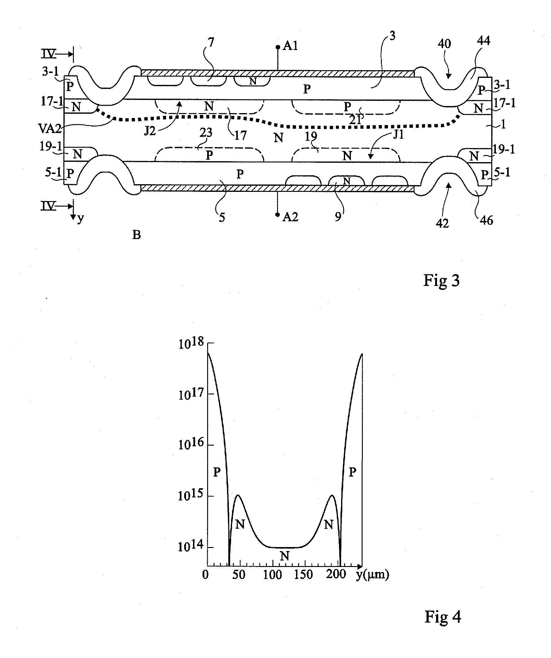
[0028]FIG. 3 is a simplified cross-section view of a bidirectional Shockley diode comprising the same elements as FIG. 2, designated with the same reference numerals. Layers 3 and 5 are formed with no masking on both sides of the structure and the other elements are formed likewise in these layers. However, this time, grooves 40, 42, filled with a glassivation 44, 46, are formed a little inside of the periphery of each component instead of being formed at the endmost periphery thereof, so that there remain unetched substrate portions beyond the groove.
[0029]In these unetched substrate portions, there thus appear, respectively on the upper surface side and on the lower surface side, portions 3-1 and 5-1 of upper and lower P layers 3 and 5. Further, at the same time as N-type buried regions 17 and 19 are formed, N-type ring-shaped buried regions 17-1 and 19-1 are formed at the component periphery, outside of grooves 40 and 42. To form ring-shaped regions 17-1, 19-1, it is sufficient t...
PUM
 Abstract
Description
Claims
Application Information