Semiconductor package and fabrication method thereof

a technology of semiconductors and packaging, applied in the direction of semiconductor devices, semiconductor/solid-state device details, electrical apparatus, etc., can solve the problems of cracking of chips, warpage on the front side of the structure, and easy warpage to so as to avoid the warpage of the backside of the overall package structure, avoid the warpage of the front side, and avoid the overall package structur

Active Publication Date: 2012-06-28
SILICONWARE PRECISION IND CO LTD
View PDF5 Cites 11 Cited by
  • Summary
  • Abstract
  • Description
  • Claims
  • Application Information

AI Technical Summary

Benefits of technology

[0019]Therefore, the first and second metal layers formed on the second surface of the encapsulant provide a rigid support to the overall package structure so as to avoid warpage of the overall package structure. Compared with the conventional structure that lacks a rigid support, the present invention avoids warpage of the backside of the overall package structure.
[0020]Further, during the fabrication process of the built-up structure, the present invention avoids warpage of the front side of the overall package structure due to the support of the first and second metal layers, thereby effectively improving the reliability of subsequent processes, avoiding the risk of cracking of the chips and improving the product yield. Moreover, the first and second metal layers facilitate heat dissipation of the overall package structure.

Problems solved by technology

However, in the fabrication process of FIG. 1C, after the chips 11 and the encapsulant 12 are completely separated from the adhesive layer 100, the overall package structure loses the rigid support of the carrier board 10 such that warpage can easily occur to the backside of the overall package structure (as shown by the dashed lines in FIG. 1C), and, even worse, cracking of the chips 11 may occur.
Further, if a wiring process is performed to the backside of the package, warpage can occur on the front side of the structure.
The above-described front and back warpage effects cannot completely offset each another, thus reducing the reliability of subsequent processes and reducing the product yield.

Method used


Image

  • Semiconductor package and fabrication method thereof
  • Semiconductor package and fabrication method thereof
  • Semiconductor package and fabrication method thereof

Examples


Embodiment Construction

[0024]The following illustrative embodiments are provided to illustrate the disclosure of the present invention along with its advantages, these and other advantages and effects being apparent to those in the art after reading this specification.

[0025]It should be noted that the drawings are not intended to limit the present invention. Various modification and variations can be made without departing from the spirit of the present invention. Further, terms such as “one”, “above”, etc. are merely for illustrative purpose and should not be construed to limit the scope of the present invention.

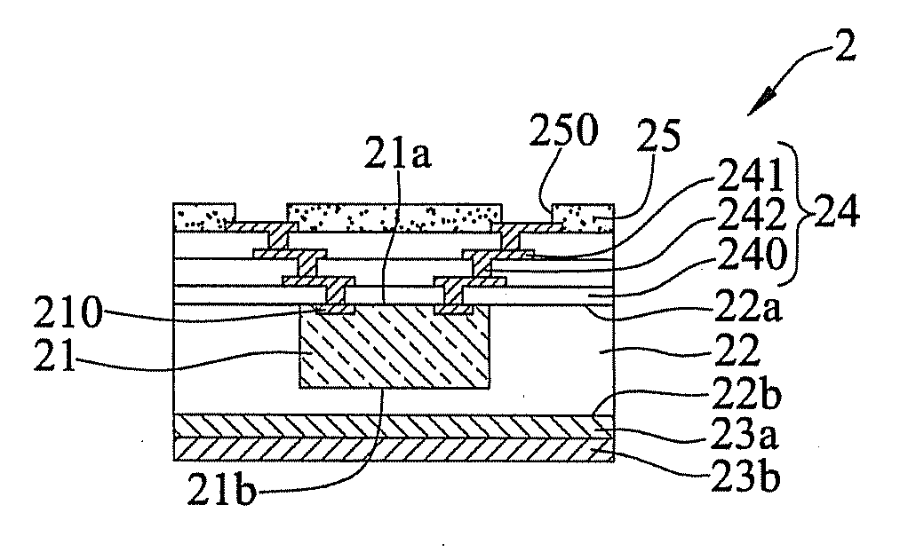
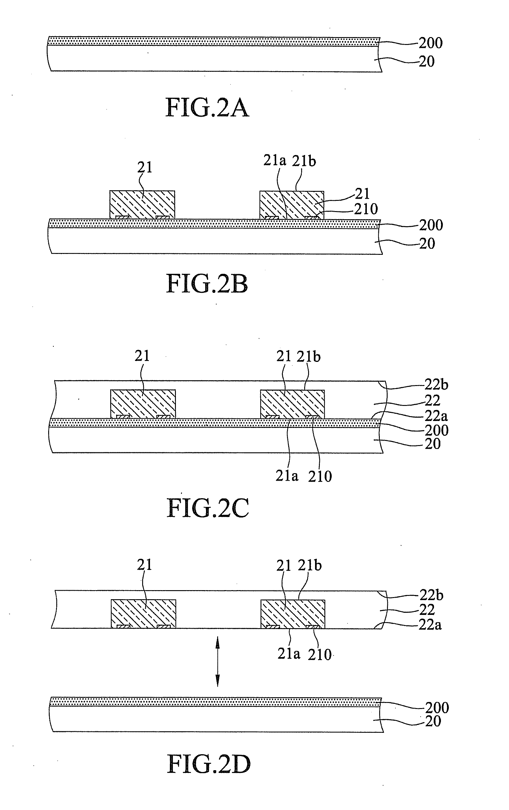
[0026]FIGS. 2A to 2G show a fabrication method of a semiconductor package according to an embodiment of the present invention.

[0027]Referring to FIG. 2A, a carrier board 20 having an adhesive layer 200 is provided. In the present embodiment, the carrier board 20 is a wafer.

[0028]Referring to FIG. 2B, a plurality of chips 21 each having an active surface 21a with a plurality of electrode pads 210 ...


PUM


Abstract

A semiconductor package includes: a chip having an active surface with a plurality of electrode pads and an inactive surface opposite to the active surface; an encapsulant encapsulating the chip and having opposite first and second surfaces, the first surface being flush with the active surface of the chip; and first and second metal layers formed on the second surface of the encapsulant, thereby providing a rigid support to the overall structure to prevent warpage and facilitating heat dissipation of the overall structure.

Description

BACKGROUND OF THE INVENTION[0001]1. Field of the Invention[0002]The present invention relates to a semiconductor package and a fabrication method thereof.[0003]2. Description of Related Art[0004]In recent years, chip scale packages (CSPs) have been developed to meet the demand for lighter, thinner and smaller semiconductor packages. Such a chip scale package has a size the same as or slightly larger than that of a chip. FIGS. 1A to 1D are cross-sectional views showing a fabrication method of a conventional chip scale package as disclosed by U.S. Pat. No. 7,202,107.[0005]Referring to FIG. 1A, a carrier board 10 having a heat-sensitive adhesive layer 100 is provided. A plurality of chips 11 each having an active surface 11a with a plurality of electrode pads 110 and an inactive surface 11b opposite to the active surface 11a is disposed on the carrier board 10 and attached to the adhesive layer 100 through the active surfaces 11a thereof.[0006]Referring to FIG. 1B, an encapsulant 12 is...

Claims


Application Information

Patent Timeline
Patent Type & Authority Applications(United States)
IPC IPC(8): H01L23/495H01L21/60H01L23/48
CPCH01L21/568H01L23/3121H01L23/36H01L23/5389H01L24/96H01L21/56H01L2224/20H01L24/19H01L24/20H01L2924/014H01L2924/3511H01L2224/04105
Inventor HUANG, JUNG-PANGHUANG, HUI-MINCHUANG, KUAN-WEILIN, CHUN-TANGJIANG, YIH-JENN
Owner SILICONWARE PRECISION IND CO LTD
Why Eureka
Try Eureka