Semiconductor device and assembling method thereof

a technology of semiconductor devices and components, applied in semiconductor devices, semiconductor/solid-state device details, electrical apparatus, etc., can solve problems such as joint damage, product reliability, and lack of flexibility, and imc has a higher rigidity and rigidity

Active Publication Date: 2012-06-28
IND TECH RES INST
View PDF4 Cites 7 Cited by
  • Summary
  • Abstract
  • Description
  • Claims
  • Application Information

AI Technical Summary

Problems solved by technology

In a flip chip bonding process, there are two conventional damage modes that influence product reliability.
One is mechanical damage, for example, during a temperature cycle reliability test, residual stress may cause joint damage due to excessive difference of thermal expansion coefficients of different materials.
Another one is that voids may appear on a solder joint due to an electromigration effect caused by a high current, which influences a joint quality and a joint strength.
On the other hand, during assembling of the solder joints or a process of high temperature reflow, intermetallic compound (IMC) can be generated on an interface of the solder joints due to the high temperature, a material hardness of the IMC is generally harder than that of the original solder joint, and the IMC has a higher rigidity and is lack of flexibility, which is liable to be damaged during the temperature cycle reliability test.

Method used


Image

  • Semiconductor device and assembling method thereof
  • Semiconductor device and assembling method thereof
  • Semiconductor device and assembling method thereof

Examples


Embodiment Construction

[0020]The disclosure is directed to a semiconductor device, which can avoid damages caused by thermal stress and an electromigration effect.

[0021]The disclosure is directed to an assembling method of a semiconductor device, where the assembled semiconductor device can avoid damages caused by thermal stress and an electromigration effect.

[0022]The disclosure is directed to the semiconductor device and the assembling method thereof, the conductive elements with different composition ratios of the intermetallic compound can resist damages caused by the thermal stresses and the electromigration effect.

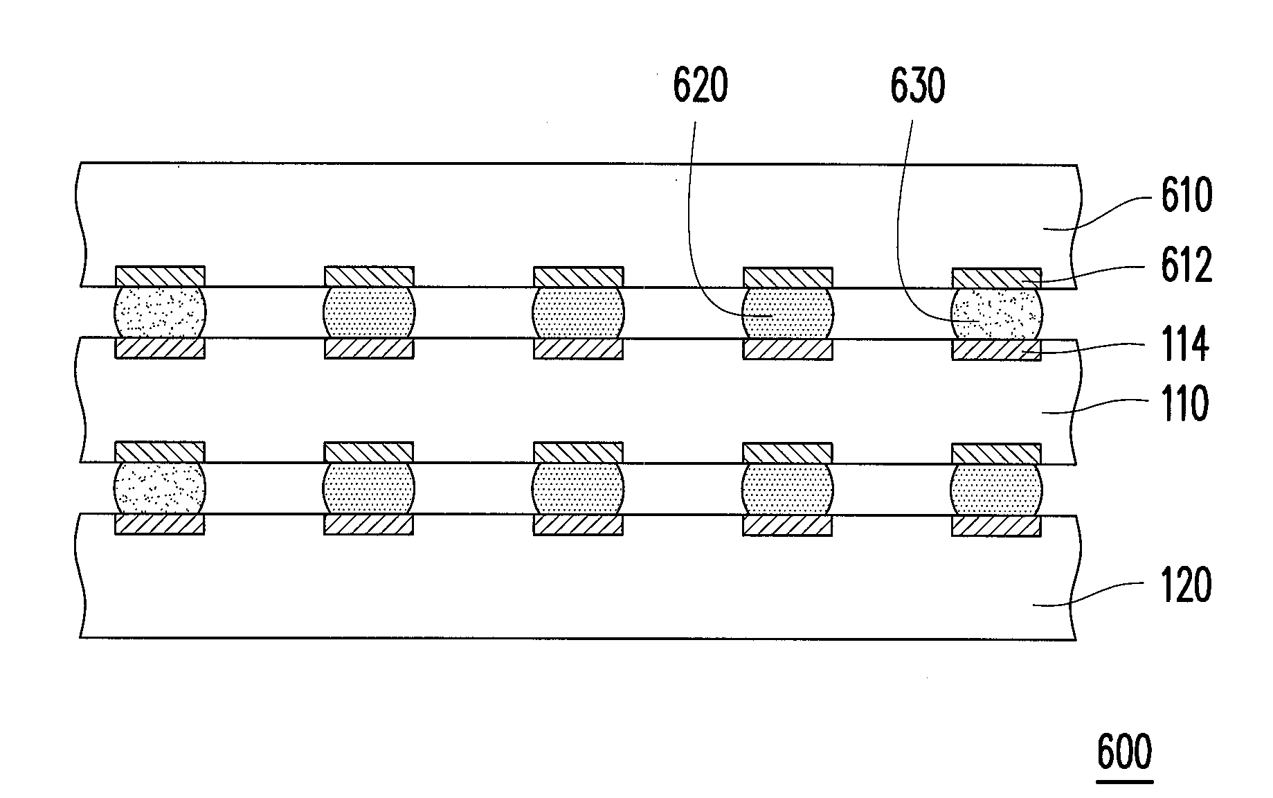
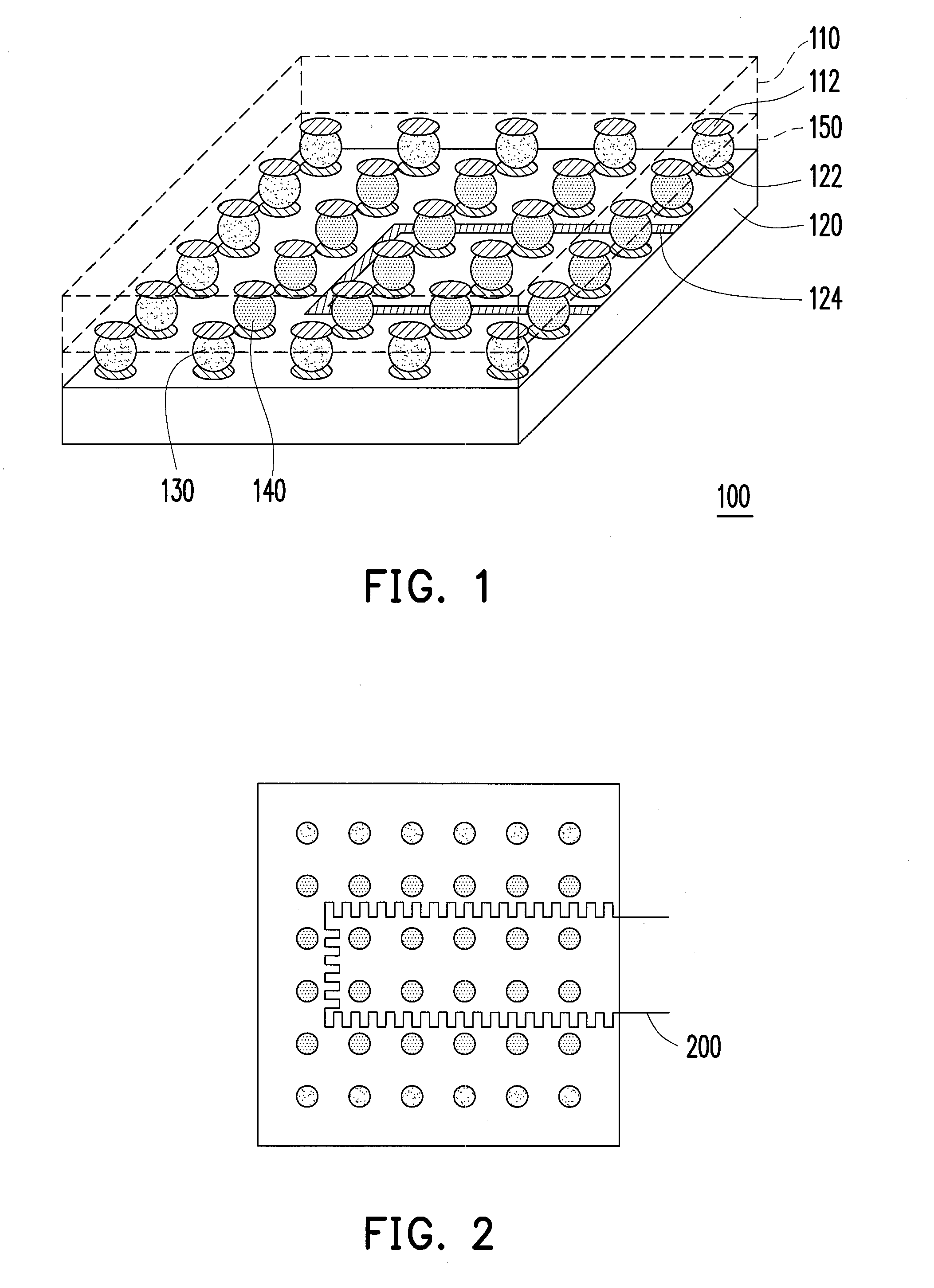
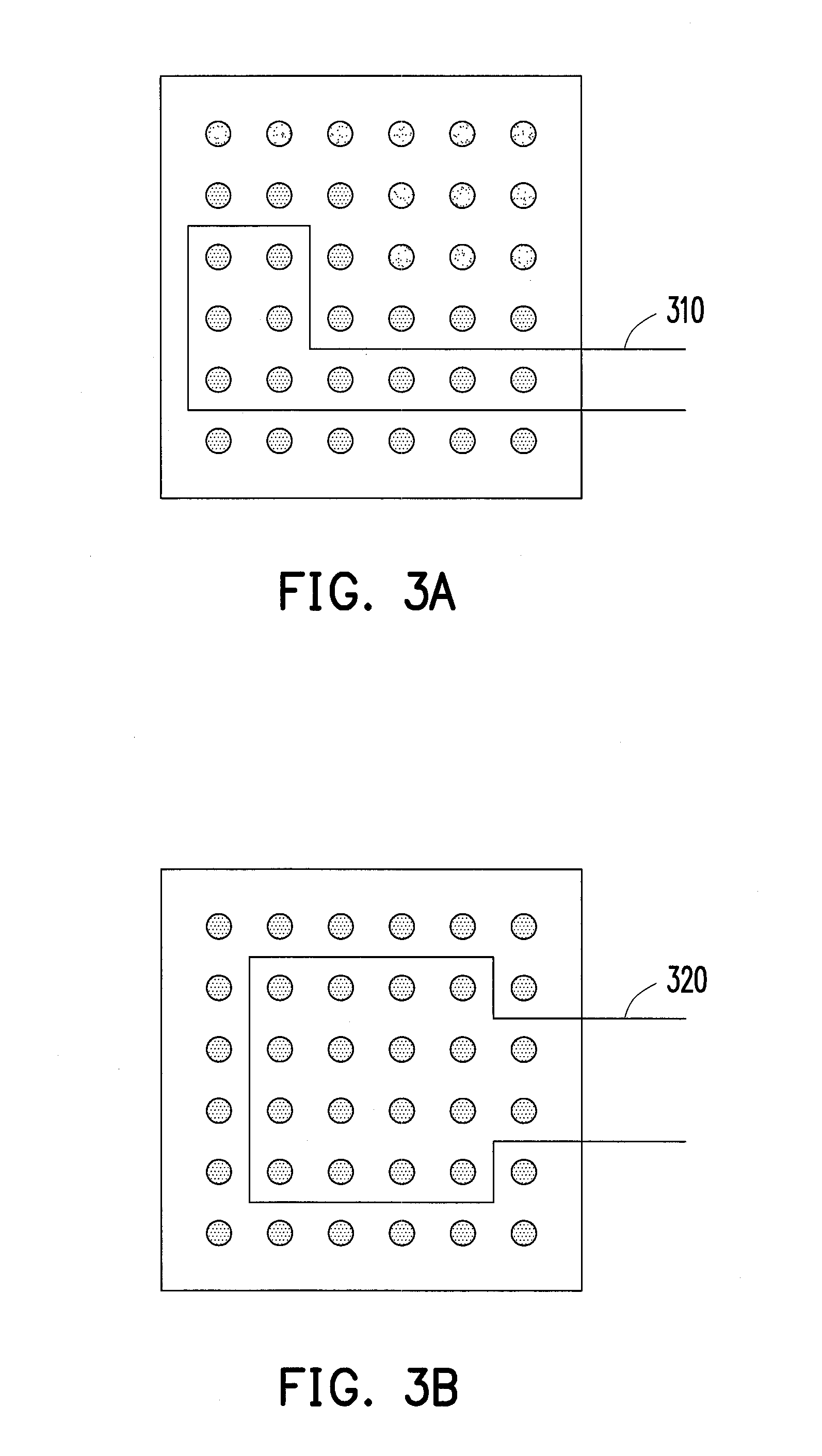
[0023]FIG. 1 is a perspective view of a semiconductor device according to an exemplary embodiment of the disclosure. Referring to FIG. 1, the semiconductor device 100 of the embodiment includes a chip 110, a carrier 120, a plurality of first conductive elements 130 and a plurality of second conductive elements 140. The chip 110 has a plurality of first pads 112. The carrier 120 has a plura...


PUM


Abstract

A semiconductor device and an assembling method thereof are provided. The semiconductor device includes a chip, a carrier, a plurality of first conductive elements and a plurality of second conductive elements. The chip has a plurality of first pads. The carrier has a plurality of second pads. The second pads correspond to the first pads. Each first conductive element is disposed between one of the first pads and one of the second pads. Each second conductive element is disposed between one of the first pads and one of the second pads. A volume ratio of intermetallic compound of the second conductive elements is greater than a volume ratio of intermetallic compound of the first conductive elements.

Description

CROSS-REFERENCE TO RELATED APPLICATION[0001]This application claims the priority benefit of Taiwan application serial no. 99146360, filed Dec. 28, 2010. The entirety of the above-mentioned patent application is hereby incorporated by reference herein and made a part of this specification.BACKGROUND[0002]1. Technical Field[0003]The disclosure relates to a semiconductor device and an assembling method thereof. Particularly, the disclosure relates to a semiconductor device using a flip chip bonding technique, and an assembling method thereof.[0004]2. Description of Related Art[0005]In a flip chip bonding process, there are two conventional damage modes that influence product reliability. One is mechanical damage, for example, during a temperature cycle reliability test, residual stress may cause joint damage due to excessive difference of thermal expansion coefficients of different materials. Another one is that voids may appear on a solder joint due to an electromigration effect cause...

Claims


Application Information

Patent Timeline
Patent Type & Authority Applications(United States)
IPC IPC(8): H01L23/48H01L21/58
CPCH01L21/563H01L2225/06513H01L24/17H01L2924/01029H01L2924/01079H01L2924/01082H01L2224/14131H01L2224/17505H01L2224/81948H01L24/81H01L2224/13111H01L2224/13144H01L2224/16145H01L2224/16225H01L2224/16507H01L2224/73204H01L2224/81191H01L2224/81193H01L2224/81224H01L2224/81234H01L2224/8181H01L2224/81815H01L2924/01033H01L2924/01047H01L2924/014H01L23/345H01L2225/06517H01L2224/92125H01L2224/14505H01L2224/0401H01L25/0657H01L24/92H01L24/73H01L24/16H01L24/14H01L2924/01327H01L2924/00013H01L2924/00014H01L2924/00H01L2224/13099H01L2224/13599H01L2224/05599H01L2224/05099H01L2224/29099H01L2224/29599H01L2224/32145H01L2924/00012H01L2224/32225H01L2924/351
Inventor LIN, YU-MINZHAN, CHAU-JIELU, SU-TSAI
Owner IND TECH RES INST
Why Eureka
Try Eureka