Electrically driven single photon source

a single photon source, electric drive technology, applied in electrical equipment, nanotechnology, nanotechnology, etc., can solve the problems of limited monochromatic, limited ion exchange rate, so as to reduce the effect of one, mitigate or eliminate on

Active Publication Date: 2012-06-28
DANMARKS TEKNISKE UNIV +1
View PDF6 Cites 10 Cited by
  • Summary
  • Abstract
  • Description
  • Claims
  • Application Information

AI Technical Summary

Benefits of technology

[0011]It may be seen as an object of the present invention to provide an improved single photon source. Preferably, the i

Problems solved by technology

However, the far field emission pattern of the required high-Q cavity is very sensitive to fabrication imperfections.
This limitation is even more serious in electrically pumped devices, because of supplementary optical losses introduced b

Method used


Image

  • Electrically driven single photon source
  • Electrically driven single photon source
  • Electrically driven single photon source

Examples


Embodiment Construction

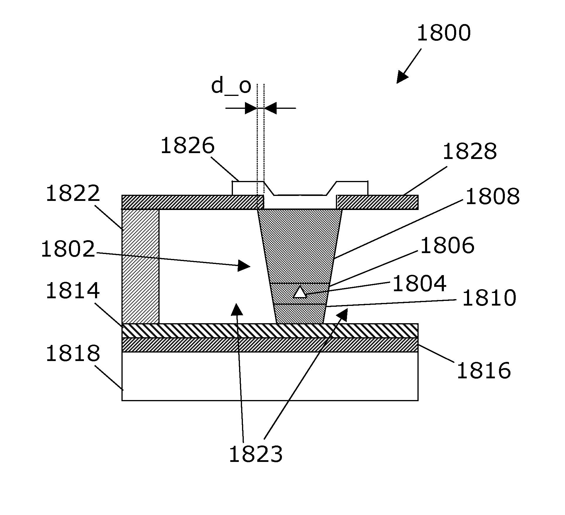
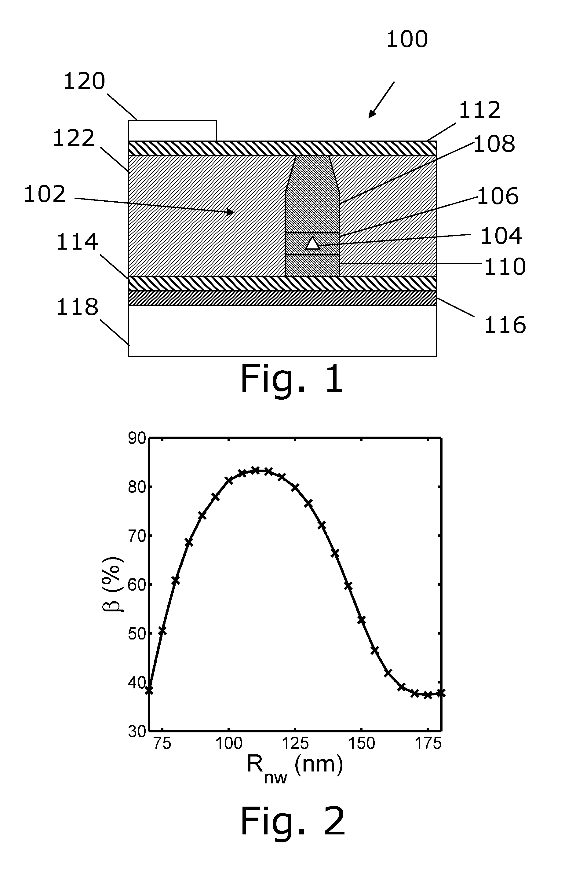
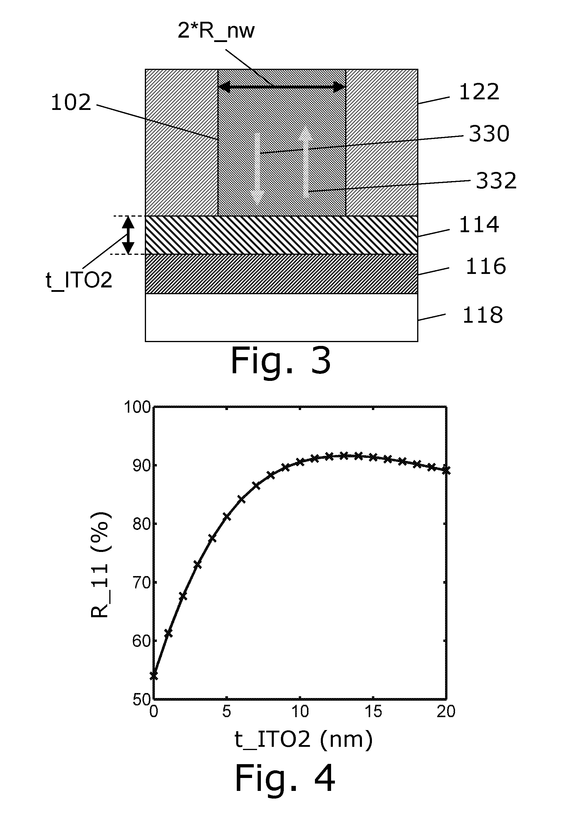
[0095]An embodiment of the invention is illustrated in FIG. 1 showing a single photon source 100 comprising a nanowire 102 which is tapered in a first end which in the figure is the upper end of the nanowire 102, the upper part of the nanowire has a top diameter which decreases towards the first end, a first electrode comprising contact pad 120 and a first indium tin oxide (ITO) layer 112, and further a second electrode comprising a second indium tin oxide (ITO) layer 114. Although both first and second electrodes comprise ITO in the present embodiment, it is understood that other materials might be comprised as well, in particular other materials which are optically transparent and electrically conducting. The nanowire 102 comprises a p-type zone 108, an n-type zone 110 and an intrinsic region 106 wherein a photon emitter 104 is embedded, the photon emitter being a quantum dot (QD) in the shown embodiment. The figure also shows a planarizing polymer 122, the planarizing polymer con...


PUM


Abstract

The present invention relates to a single photon source 1800 comprising a tapered nanowire 1802, where the nanowire 1802 is made of a semiconductor material, a first electrode 1828 and second electrode 1814, where the electrodes are electrically coupled to a photon emitter 1804 embedded in the nanowire 1802 and wherein the photon emitter 1804 is capable of emitting a single photon when an activation voltage is applied between the electrodes. In advantageous embodiments of the invention, the nanowire is encircled by air or vacuum, such that advantage can be taken of the resultant large ratio between a refractive index of the nanowire and the encircling material, air. Another advantageous feature might be that the first and second electrodes are optically transparent, such that they can be used as part of a reflective element or anti-reflective element.

Description

FIELD OF THE INVENTION[0001]The invention relates to a single photon source, and in particular to an electrically driven single photon source.BACKGROUND OF THE INVENTION[0002]Major efforts have been devoted over the last ten years to the development of light emitters able to emit photons one by one in a deterministic way. Such emitters, known as single photon sources (SPS), are key devices in quantum cryptography, and could find applications in quantum information processing or metrology (standards for the energy or the light flux).[0003]The spontaneous far-field radiation pattern of a single photon emitter is naturally omni-directional. In view of practical applications, it is therefore essential to tailor this radiation pattern so as to ensure, e.g., a directional emission in free space, or a good coupling to an optical channel, such as an optical fibre. Generally speaking, such a tailoring is performed through an engineering of the electromagnetic environment of the emitter.[0004...

Claims


Application Information

Patent Timeline
IPC IPC(8): H05B37/00H01L33/04B82Y99/00
CPCH01L33/06B82Y20/00
Inventor GREGERSEN, NIELSCLAUDON, JULIENGERARD, JEAN-MICHEL
Owner DANMARKS TEKNISKE UNIV
Why Eureka
Try Eureka