Methods and systems for in-situ pyrometer calibration

a pyrometer and in-situ technology, applied in the direction of optical radiation measurement, semiconductor/solid-state device testing/measurement, instruments, etc., can solve the problems of inability to accurately measure and the inability to achieve the actual temperature of the wafer carrier and the in-process wafer

a pyrometer and in-situ technology, applied in the direction of optical radiation measurement, semiconductor/solid-state device testing/measurement, instruments, etc., can solve the problems of inability to accurately measure and the inability to achieve the actual temperature of the wafer carrier and the in-process wafer

US20120170609A1Active Publication Date: 2012-07-05VEECO INSTR

Image

  • Methods and systems for in-situ pyrometer calibration
  • Methods and systems for in-situ pyrometer calibration

Examples


Embodiment Construction

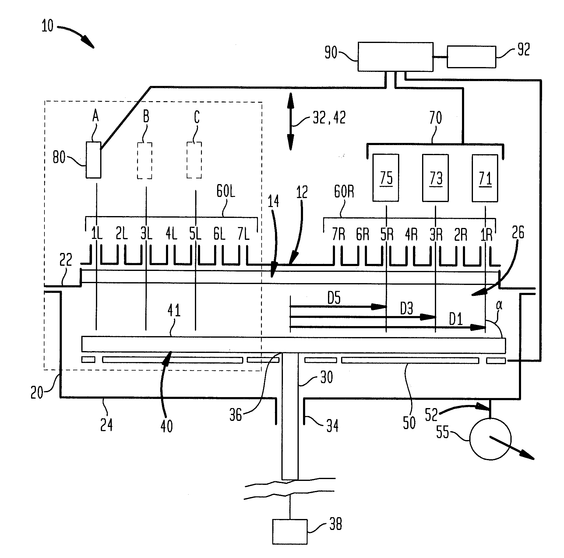
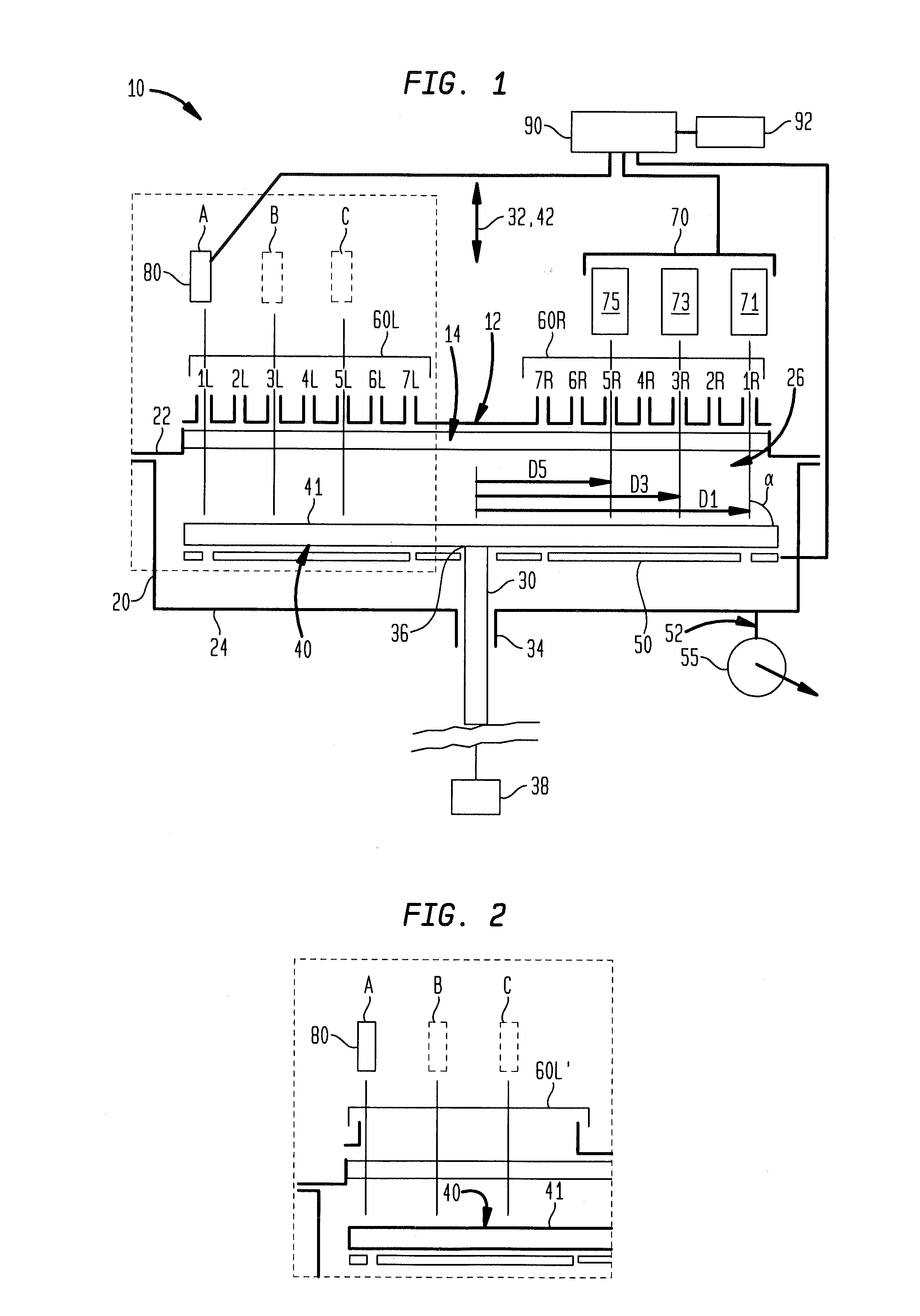
[0025]Referring to FIG. 1, a chemical vapor deposition apparatus 10 in accordance with one embodiment of the invention includes a reaction chamber 12 having a gas inlet manifold 14 arranged at one end of the chamber 12. The end of the chamber 12 having the gas inlet manifold 14 is referred to herein as the “top” end of the chamber 12. This end of the chamber typically, but not necessarily, is disposed at the top of the chamber in the normal gravitational frame of reference. Thus, the downward direction as used herein refers to the direction away from the gas inlet manifold 14; whereas the upward direction refers to the direction within the chamber, toward the gas inlet manifold 14, regardless of whether these directions are aligned with the gravitational upward and downward directions. Similarly, the “top” and “bottom” surfaces of elements are described herein with reference to the frame of reference of chamber 12 and manifold 14.

[0026]The chamber 12 has a cylindrical wall 20 that e...


PUM


Abstract

A method of in-situ pyrometer calibration for a wafer treatment reactor such as a chemical vapor deposition reactor desirably includes the steps of positioning a calibrating pyrometer at a first calibrating position and heating the reactor until the reactor reaches a pyrometer calibration temperature. The method desirably further includes rotating the support element about the rotational axis, and while the support element is rotating about the rotational axis, obtaining first operating temperature measurements from a first operating pyrometer installed at a first operating position, and obtaining first calibrating temperature measurements from the calibration pyrometer. Both the calibrating pyrometer and the first operating pyrometer desirably are adapted to receive radiation from a first portion of a wafer support element at a first radial distance from a rotational axis of the wafer support element.

Description

CROSS-REFERENCE TO RELATED APPLICATIONS[0001]The present application claims the benefit of the filing date of U.S. Provisional Patent Application Ser. No. 61 / 428,494, filed Dec. 30, 2010, the disclosure of which is hereby incorporated by reference herein.BACKGROUND OF THE INVENTION[0002]The present invention relates to wafer processing apparatus, to pyrometer calibration systems for use in such processing apparatus, and to methods of in-situ pyrometer calibration.[0003]Many semiconductor devices are formed by processes performed on a substrate. The substrate typically is a slab of a crystalline material, commonly referred to as a “wafer.” Typically, a wafer is formed by growing a large crystal and slicing the crystal into the shape of a disc. One common process performed on such a wafer is epitaxial growth.[0004]For example, devices formed from compound semiconductors such as III-V semiconductors typically are formed by growing successive layers of the compound semiconductor using m...

Claims


Application Information

Patent Timeline
05 Jul 2012
Publication
US20120170609A1
IPC
G01K15/00
CPC
G01J5/0003; G01J2005/0048; G01J5/0007; G01J5/80; G01J5/00; H01L22/00
Inventors
GURARY, ALEXANDER I.; BOGUSLAVSKIY, VADIM