Thin film deposition using microwave plasma

a thin film and microwave technology, applied in the direction of plasma technique, chemical vapor deposition coating, coating, etc., can solve the problems of large input power drop across the plasma sheath, dark space, difficulty in maintaining homogeneity during scale up

Inactive Publication Date: 2012-07-05
APPLIED MATERIALS INC
View PDF12 Cites 382 Cited by
  • Summary
  • Abstract
  • Description
  • Claims
  • Application Information

AI Technical Summary

Problems solved by technology

One drawback of using RF plasma is that a large portion of the input power is dropped across the plasma sheath (dark space).
In the past, the main drawback associated with microwave source technology in the vacuum coating industry was the difficulty in maintaining homogeneity during scale up from small wafer processing to very large area substrate processing.

Method used


Image

  • Thin film deposition using microwave plasma
  • Thin film deposition using microwave plasma
  • Thin film deposition using microwave plasma

Examples


Embodiment Construction

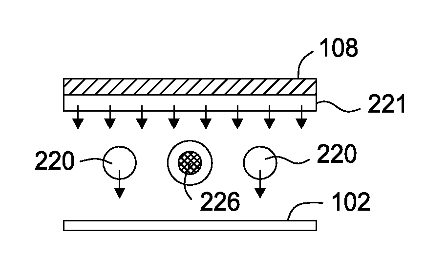
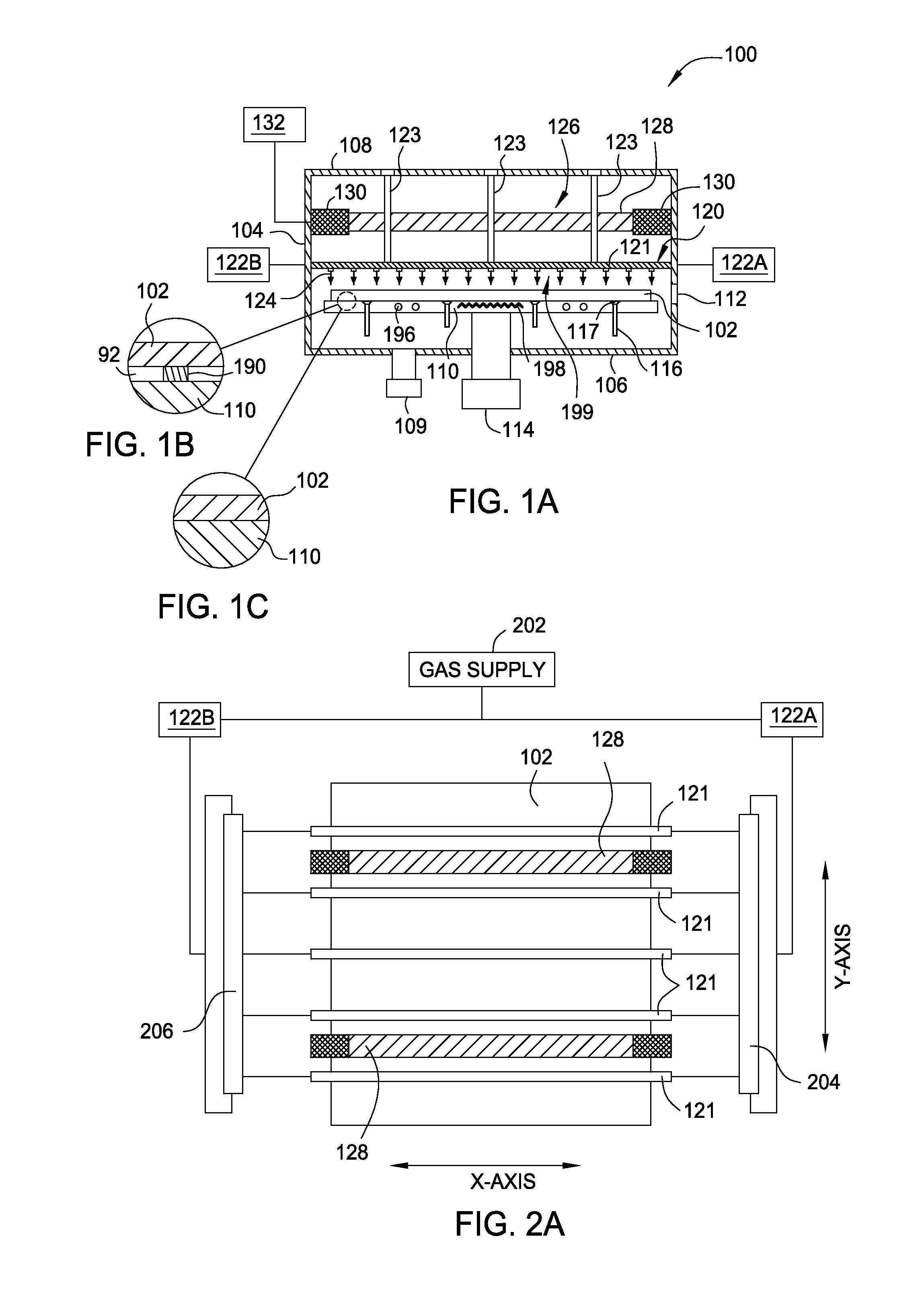
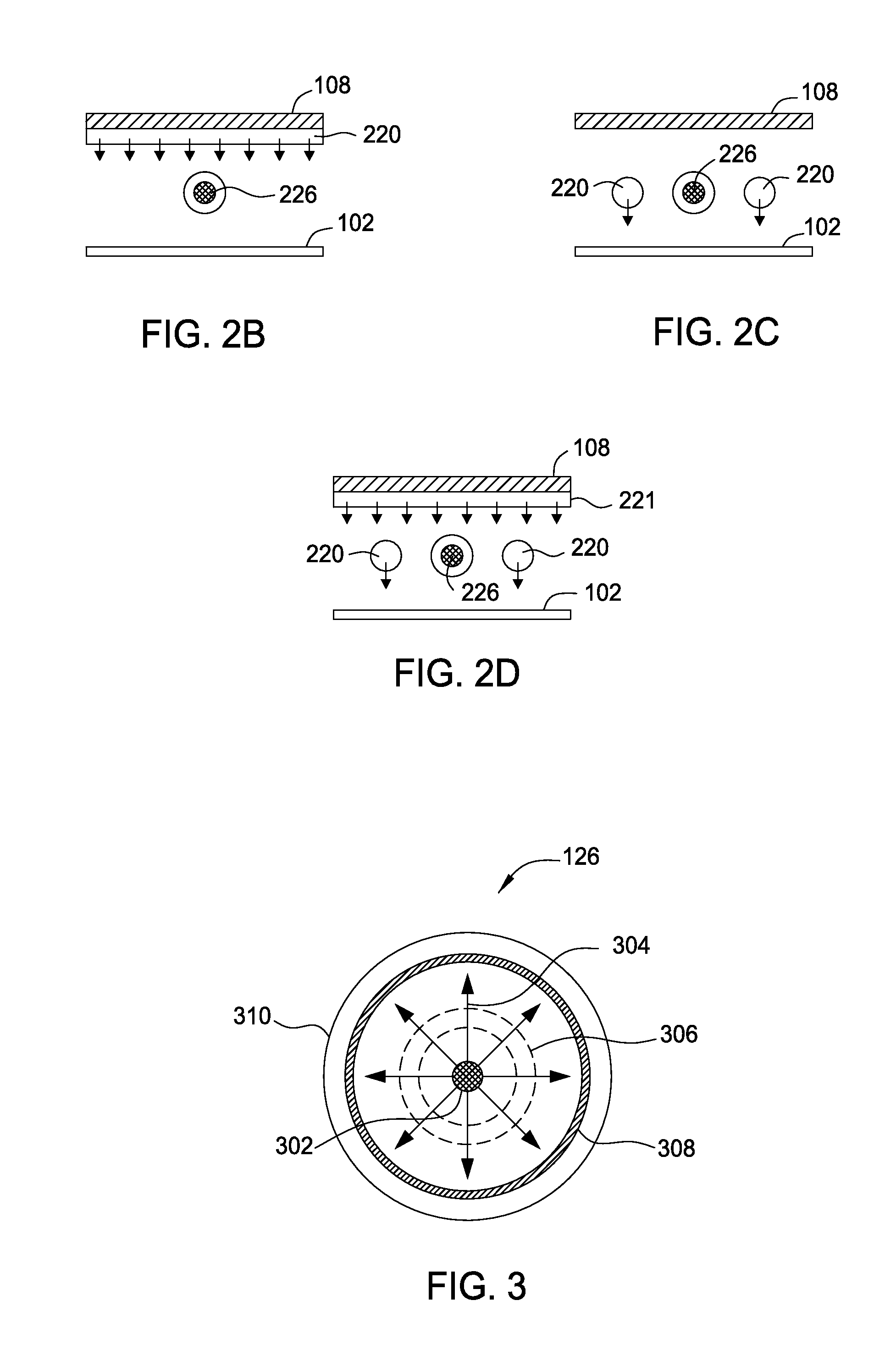
[0021]Embodiments of the present invention provide deposition processes for a silicon-containing dielectric layer (e.g., SiN) using an improved microwave-assisted CVD chamber. The improved microwave-assisted CVD chamber includes a gas feeding source and a coaxial microwave source that are positioned in a parallel relationship with a substrate susceptor upon which a substrate is placed. The gas feeding source may be located between the coaxial microwave source and the substrate susceptor. The gas feeding source may include an array of gas feeding lines which are arranged parallel and longitudinally spaced from each other. The coaxial microwave source may include a single or plural linear microwave generator which may be arranged in a parallel relationship to the longitudinal direction of the gas feeding lines. By using the inventive apparatus with microwave plasma source, good quality of CVD film can be obtained without the need of substrate susceptors using expensive heating element...


PUM

PropertyMeasurementUnit
temperatureaaaaaaaaaa
chamber pressureaaaaaaaaaa
distanceaaaaaaaaaa

Abstract

Embodiments of the present invention generally provide deposition processes for a silicon-containing dielectric layer using an improved microwave-assisted CVD chamber. In one embodiment, a method of processing a substrate in a processing chamber is provided. The method generally includes applying a microwave power to an antenna coupled to a microwave source disposed within the processing chamber, wherein the microwave source is disposed relatively above a gas feeding source configured to provide a gas distribution coverage covering substantially an entire surface of the substrate, and exposing the substrate to a microwave plasma generated from a processing gas provided by the gas feeding source to deposit a silicon-containing layer on the substrate at a temperature lower than about 200 degrees Celsius, the microwave plasma using a microwave power of about 500 milliWatts / cm2 to about 5,000 milliWatts / cm2 at a frequency of about 1 GHz to about 10 GHz.

Description

CROSS-REFERENCE TO RELATED APPLICATIONS[0001]This application claims benefit of U.S. provisional patent application Ser. No. 61 / 428,837, filed Dec. 30, 2010, which is herein incorporated by reference.BACKGROUND OF THE INVENTION[0002]1. Field of the Invention[0003]Embodiments of the present invention generally relate to deposition processes for a silicon-containing dielectric layer using an improved microwave-assisted CVD chamber.[0004]2. Description of the Related Art[0005]In the manufacture of integrated circuits, chemical vapor deposition (CVD) processes are often used for deposition or etching of various material layers. Examples of common CVD technologies include thermal CVD, low pressure CVD (LPCVD), plasma-enhanced CVD (PECVD), microwave plasma-assisted CVD, atmospheric pressure CVD, and the like. Conventional thermal CVD processes supply reactive compounds to the substrate surface where heat-induced chemical reactions take place to produce a desired layer. Plasma enhanced che...

Claims


Application Information

Patent Timeline
Patent Type & Authority Applications(United States)
IPC IPC(8): C23C16/511
CPCC23C16/345C23C16/45578C23C16/511H01J37/3244H01J37/32192H01J37/3222C23C16/545H01L21/205
Inventor WON, TAE KYUNGNOMINANDA, HELINDACHO, SEON-MEECHOI, SOO YOUNGPARK, BEOM SOOWHITE, JOHN M.ANWAR, SUHAILKUDELA, JOZEF
Owner APPLIED MATERIALS INC
Why Eureka
Try Eureka