

Substrate processing method and substrate processing apparatus
- Summary
- Abstract
- Description
- Claims
- Application Information
AI Technical Summary
Benefits of technology
Problems solved by technology
Method used
Image

Examples
first embodiment
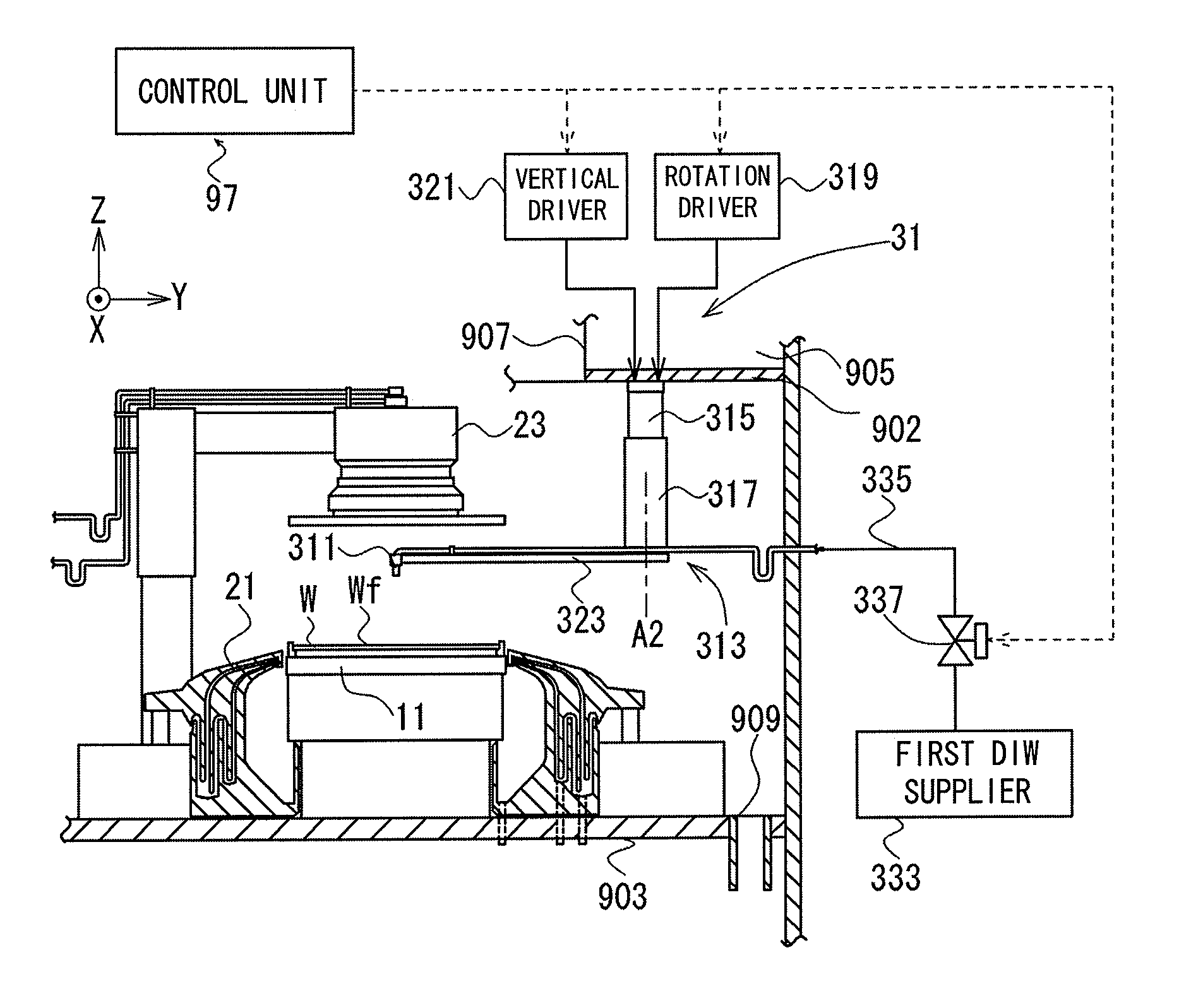
[0056]FIGS. 3, 4 and 5 are diagrams showing a schematic construction of a substrate processing apparatus 9 according to this invention. FIG. 3 is a front view of the substrate processing apparatus 9, FIG. 4 is a sectional view taken along a line B1-B1 indicted by arrows of the substrate processing apparatus 9 in FIG. 3. FIG. 5 is a side view of the substrate processing apparatus 9 in FIG. 3 when viewed in a direction of an arrow B2. This apparatus is a single-substrate processing apparatus used in a cleaning process for removing contaminants such as particles (hereinafter, referred to as “particles and the like”) adhering to a substrate W such as a semiconductor substrate (hereinafter, merely referred to as a “substrate W”).
[0057]Note that a coordinate system with a Z axis extending in a vertical direction and an XY plane as a horizontal plane is appropriately attached to the respective drawings to make a directional relationship clear. Further, in each coordinate system, a pointing...
second embodiment
[0194]Next, a second embodiment of the substrate processing apparatus according to this invention is described. This second embodiment largely differs from the first embodiment in that the substrate cooling step of cooling a substrate W is performed before the solidified material forming step.
[0195]Note that since the construction of the second embodiment is basically identical to the substrate processing apparatus 9 and the processing units 91 shown in FIGS. 3 to 14, it is denoted by the same reference numerals and not described in the following description.
[0196]Also in this second embodiment, a substrate loading step of loading a substrate W into a processing unit 91 (S201) and a preparation step of preparing the DIW as the solidification liquid in an excessively cooled state (S202) are performed as in the first embodiment.
[0197]Subsequently, a substrate cooling step of cooling the substrate W (Step S203) is performed on a substrate under surface Wb. First, in response to an oper...
third embodiment
[0216]Next, a third embodiment of the substrate processing apparatus according to this invention is described. This third embodiment largely differs from the second embodiment in that the substrate cooling step is continued during the solidified material forming step to vibrate the liquid coolant.
[0217]Note that since the construction of the third embodiment is basically identical to the substrate processing apparatus 9 and the processing units 91 shown in FIGS. 3 to 14, it is denoted by the same reference numerals and not described in the following description.
[0218]Also in this third embodiment, a substrate loading step of loading a substrate W into a processing unit 91 (S201) and a preparation step of preparing the DIW as the solidification liquid in an excessively cooled state (S202) are performed as in the second embodiment.
[0219]Subsequently, a substrate cooling step of cooling the substrate W (Step S203) is performed on a substrate under surface Wb. First, in response to an o...
PUM
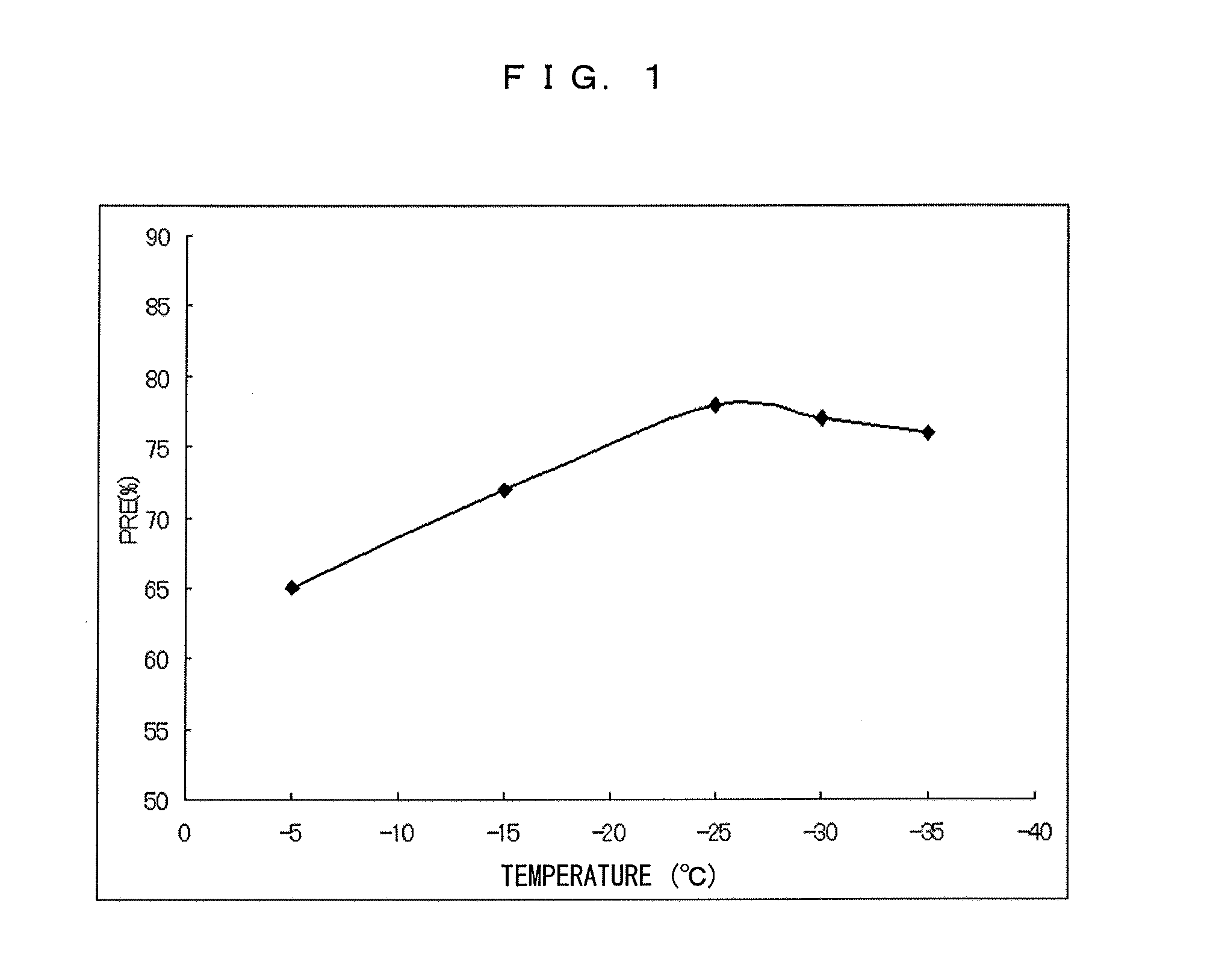
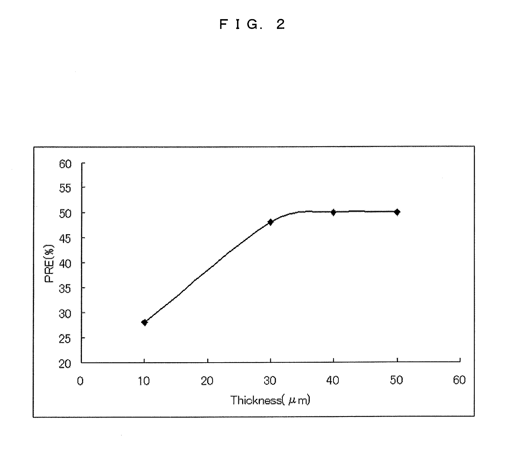
| Property | Measurement | Unit |
|---|---|---|
| Temperature | aaaaa | aaaaa |
| Time | aaaaa | aaaaa |
| Thickness | aaaaa | aaaaa |
Abstract
Description
Claims
Application Information