Waveguide electro-absorption modulator

Active Publication Date: 2012-07-12
ORACLE INT CORP
View PDF6 Cites 10 Cited by
  • Summary
  • Abstract
  • Description
  • Claims
  • Application Information

AI Technical Summary

Benefits of technology

[0016]Another embodiment provides an electro-absorption modulator. This electro-absorption modulator includes a substrate, and an optical waveguide, disposed on the substrate, having a slot approximately coaxial with a midline of the optical waveguide. Note that the slot has a depth approximately equal to a height of the optical waveguide and a width that is less than a width of the optical waveguide, where two regions of the optical waveguide external to the slot along a width of the optical waveguide are doped. Moreover, a semiconductor layer is disposed on the substrate and substantially fills the slot. Furthermore, first and second intervening layers in the ele

Problems solved by technology

It is complicated to construct efficient light modulators because the electro-optic effect in silicon (Si) is weak.
One problem associated with this approach is that the light modulator is f

Method used


Image

  • Waveguide electro-absorption modulator
  • Waveguide electro-absorption modulator
  • Waveguide electro-absorption modulator

Examples


Example

[0029]Note that like reference numerals refer to corresponding parts throughout the drawings. Moreover, multiple instances of the same part are designated by a common prefix separated from an instance number by a dash.

DETAILED DESCRIPTION

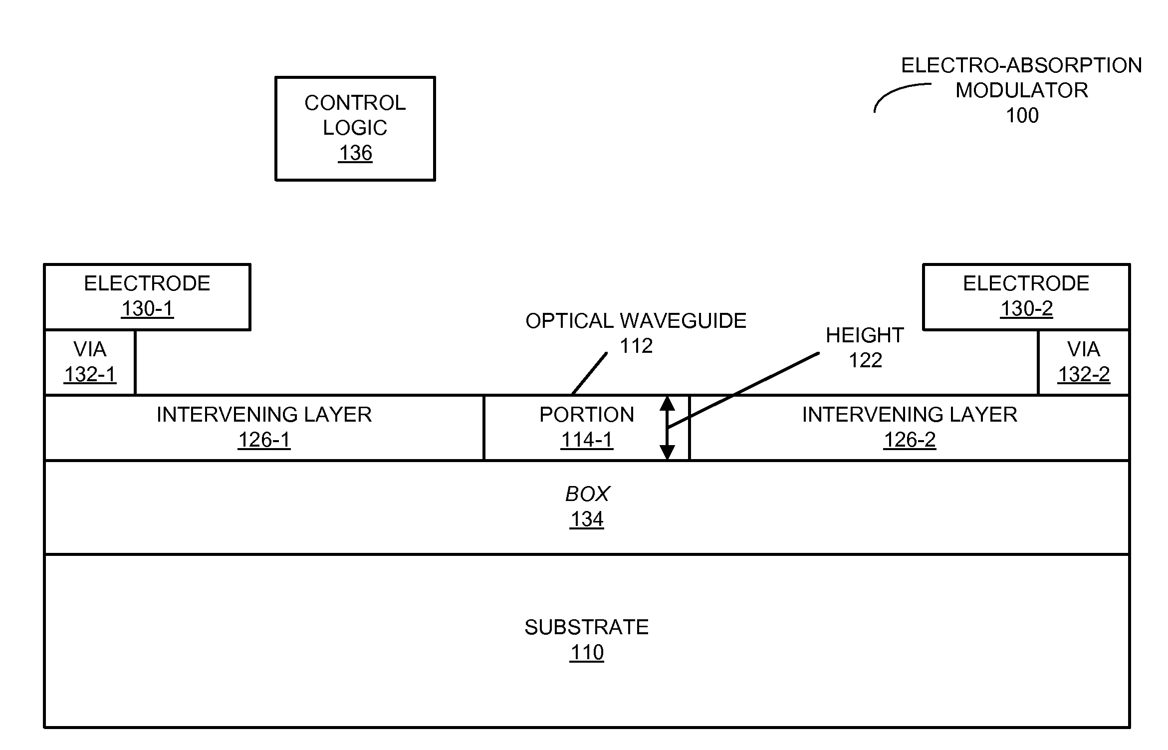
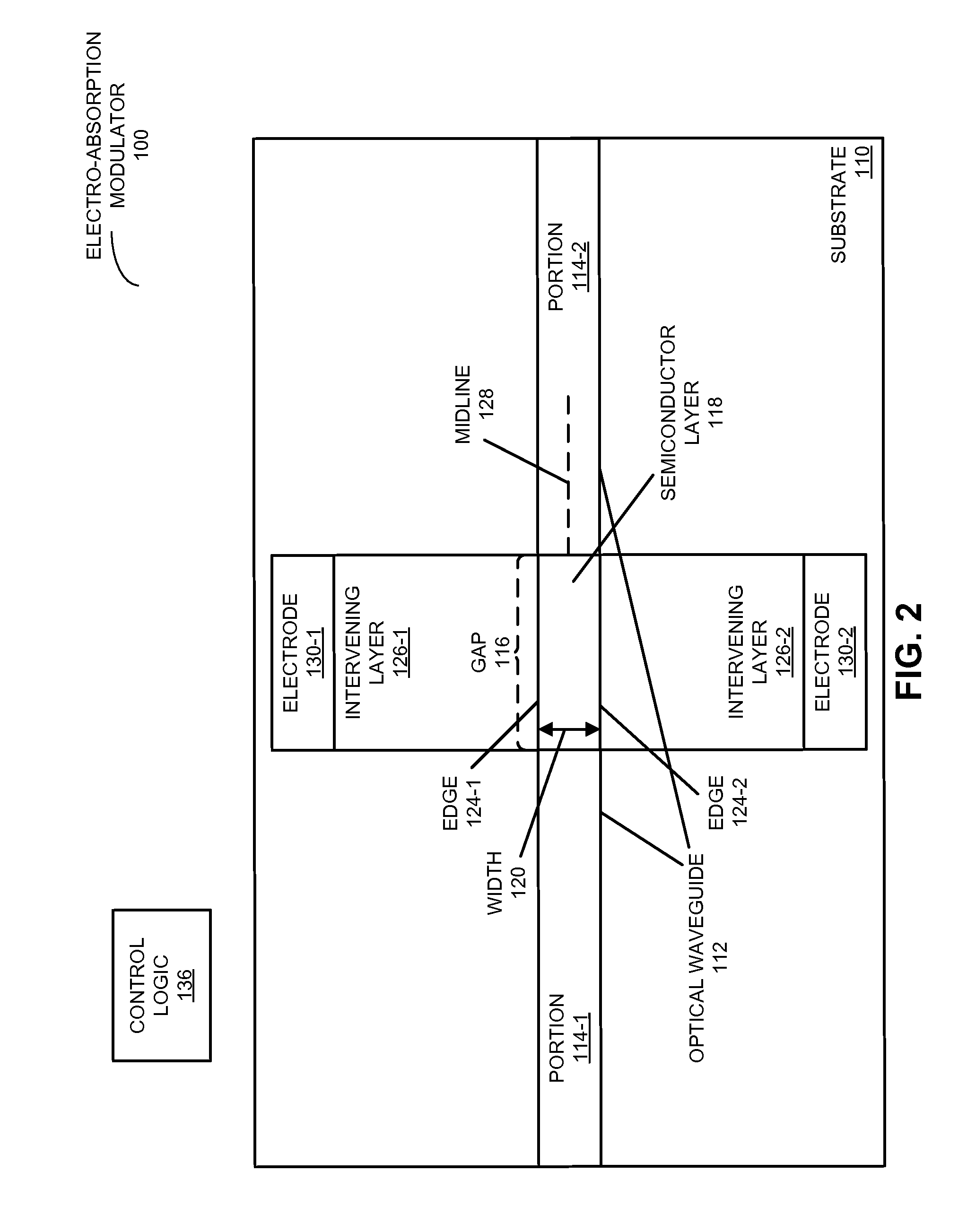
[0030]Embodiments of an electro-absorption modulator, a system that includes the electro-absorption modulator, and a method for selectively optically modulating an optical signal using the electro-absorption modulator are described. During operation, the optical signal is conveyed, using an optical waveguide in the electro-absorption modulator, to a semiconductor layer that substantially fills a gap between two portions of the optical waveguide. Then, the optical signal is electro-absorption modulated by selectively applying a voltage to electrodes that produces an electric field, approximately perpendicular to the midline of the optical waveguide, in the semiconductor layer. These electrodes are coupled to the edges of the semiconductor layer at th...


PUM


Abstract

During operation of an electro-absorption modulator, an optical signal is conveyed, using an optical waveguide in the electro-absorption modulator, to a semiconductor layer that substantially fills a gap between two portions of the optical waveguide. Then, the optical signal is electro-absorption modulated by selectively applying a voltage to electrodes that produces an electric field, approximately perpendicular to the midline of the optical waveguide, in the semiconductor layer. These electrodes are coupled to the edges of the semiconductor layer at the periphery along the width of the semiconductor layer by intervening layers. Furthermore, the intervening layers include a material that has a lower index of refraction than the semiconductor layer, and a lower optical absorption than the electrodes.

Description

GOVERNMENT LICENSE RIGHTS[0001]The United States Government has a paid-up license in this invention and the right in limited circumstances to require the patent owner to license others on reasonable terms as provided for by the terms of Agreement No. HR0011-08-9-0001 awarded by the Defense Advanced Research Projects Administration.BACKGROUND[0002]1. Field[0003]The present disclosure generally relates to electro-absorption-modulator devices. More specifically, the present disclosure relates to a waveguide electro-absorption-modulator device.[0004]2. Related Art[0005]Silicon photonics is a promising new technology that can potentially provide low-power, high-bandwidth and low-latency interconnects in future computing systems. However, in order to implement silicon photonic links, efficient light modulators are needed. It is complicated to construct efficient light modulators because the electro-optic effect in silicon (Si) is weak. As a consequence, a number of alternate light-modulat...

Claims


Application Information

Patent Timeline
IPC IPC(8): G02F1/01
CPCG02F2001/0157G02F1/025G02F1/0157
Inventor ZHENG, XUEZHECUNNINGHAM, JOHN E.KRISHNAMOORTHY, ASHOK V.
Owner ORACLE INT CORP
Why Eureka
Try Eureka