Semiconductor device and method for manufacturing semiconductor device

Inactive Publication Date: 2012-07-19
SHARP KK
View PDF8 Cites 9 Cited by
  • Summary
  • Abstract
  • Description
  • Claims
  • Application Information

AI Technical Summary

Benefits of technology

[0021]In addition, the conventional complementary logic circuit substrate cannot solve the problem that the electrode material and the organic semiconductor are in contact with each other with poor adhesiveness due to low affinity with each other, so that the efficiency in the carrier injection and the carrier extraction is lowered and the contact resistance is accordingly increased.
[0034]As described above, in the semiconductor device in accordance with the present invention, (i) the source electrodes and the drain electrodes are made from the same electrode material and (ii) layer for enhancing electric charge transfer is provided between each of the source electrodes and corresponding one of the organic semiconductor layers and between each of the drain electrodes and corresponding one of the organic semiconductor layers. This makes it possible to improve characteristics such as a mobility and a contact resistance while preventing an increase in the fabrication cost.

Problems solved by technology

However, the organic transistor is inferior yet to an inorganic semiconductor device in terms of electric properties such as (i) a carrier mobility of an organic semiconductor material and (ii) a contact resistance between an organic semiconductor and a source electrode and between the organic semiconductor and a drain electrode.
That is, since the organic semiconductor does not have a carrier in the semiconductor material, injection and control of a carrier by means of doping is difficult, unlike in the inorganic semiconductor organic transistor.
The contact resistance in the interface between the source electrode and the organic semiconductor layer therefore has a serious impact on the transistor characteristics.
This is why the reduction in contact resistance in the interface between the drain electrode and the organic semiconductor layer is an equally major problem to be solved.
Another cause is a problem resulting from a physically poor adhesiveness due to a low affinity between different types of materials such as a metal and an organic material.
However, fabrication of the logic circuit by use of an organic transistor has such problems as a complexity in the fabrication process and a high fabrication cost due to having more steps in film formation and patterning as compared with fabrication of a device employing an inorganic semiconductor.

Method used


Image

  • Semiconductor device and method for manufacturing semiconductor device
  • Semiconductor device and method for manufacturing semiconductor device
  • Semiconductor device and method for manufacturing semiconductor device

Examples


embodiment 1

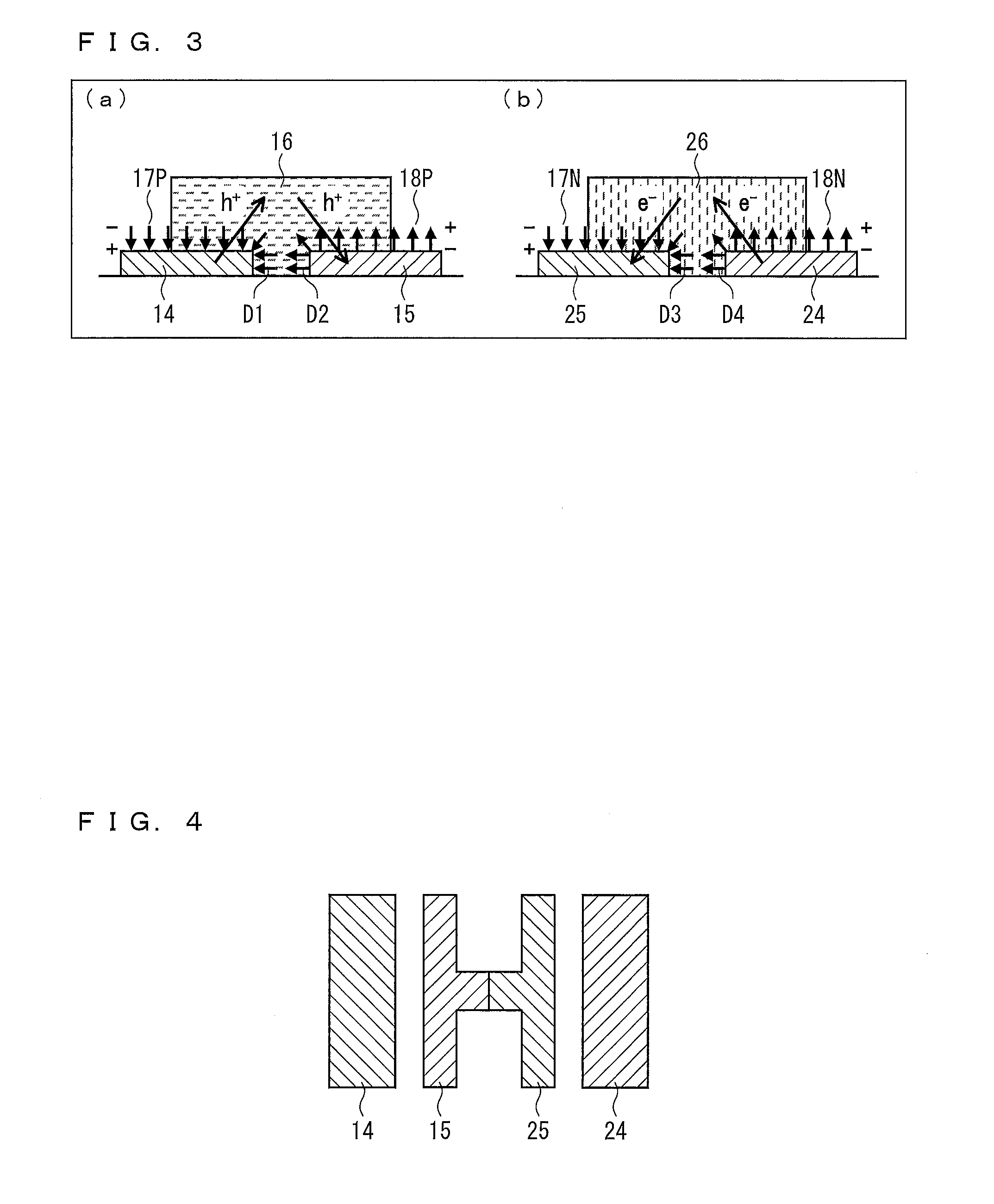
[0051]The following description will discuss, with reference to FIGS. 1 through 7, an embodiment of a semiconductor device in accordance with the present invention.

[0052](Configuration of Semiconductor Device and Organic Transistors)

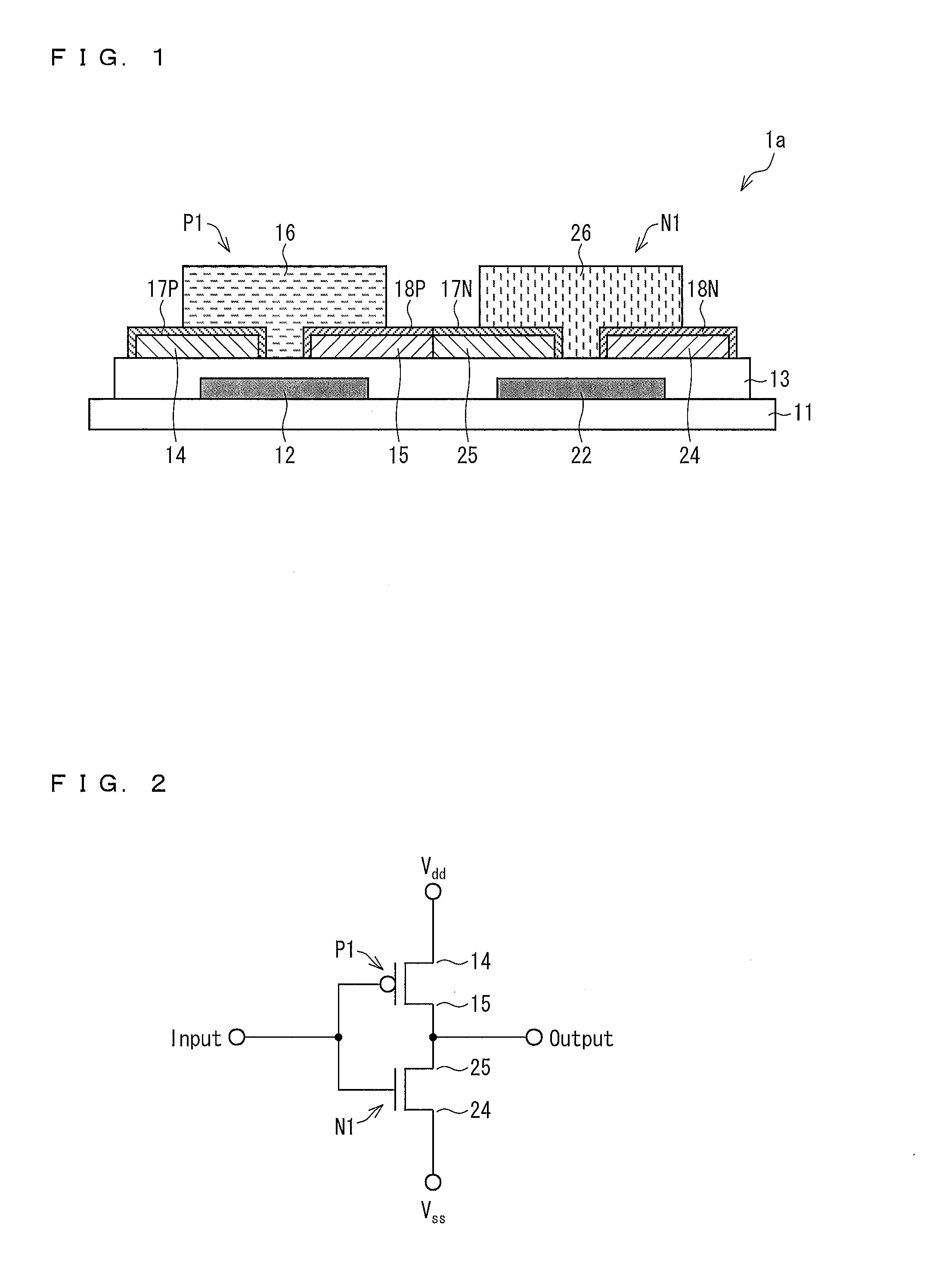
[0053]FIG. 1 is a cross-sectional view illustrating a schematic configuration of a semiconductor device of the present embodiment. As illustrated in FIG. 1, a semiconductor device 1a includes a p-type organic transistor (hereinafter simply referred to as a p-type transistor) P1 and an n-type organic transistor (hereinafter simply referred to as an n-type transistor) N1, which are provided on a same substrate 11. Each of the p-type transistor P1 and the n-type transistor N1 is a field-effect transistor whose semiconductor layer is made from an organic material.

[0054]The p-type transistor P1 is a bottom gate transistor, and includes (i) the substrate 11, (ii) a gate electrode (first gate electrode) 12 which is for the p-type transistor and is provided on t...

embodiment 2

[0144]The following description will discuss, with reference to FIGS. 8 through 11, another embodiment of the semiconductor device in accordance with the present invention. For convenience, the same reference signs will be given to members having the respective same functions as those used in Embodiment 1, and descriptions on such members will be omitted.

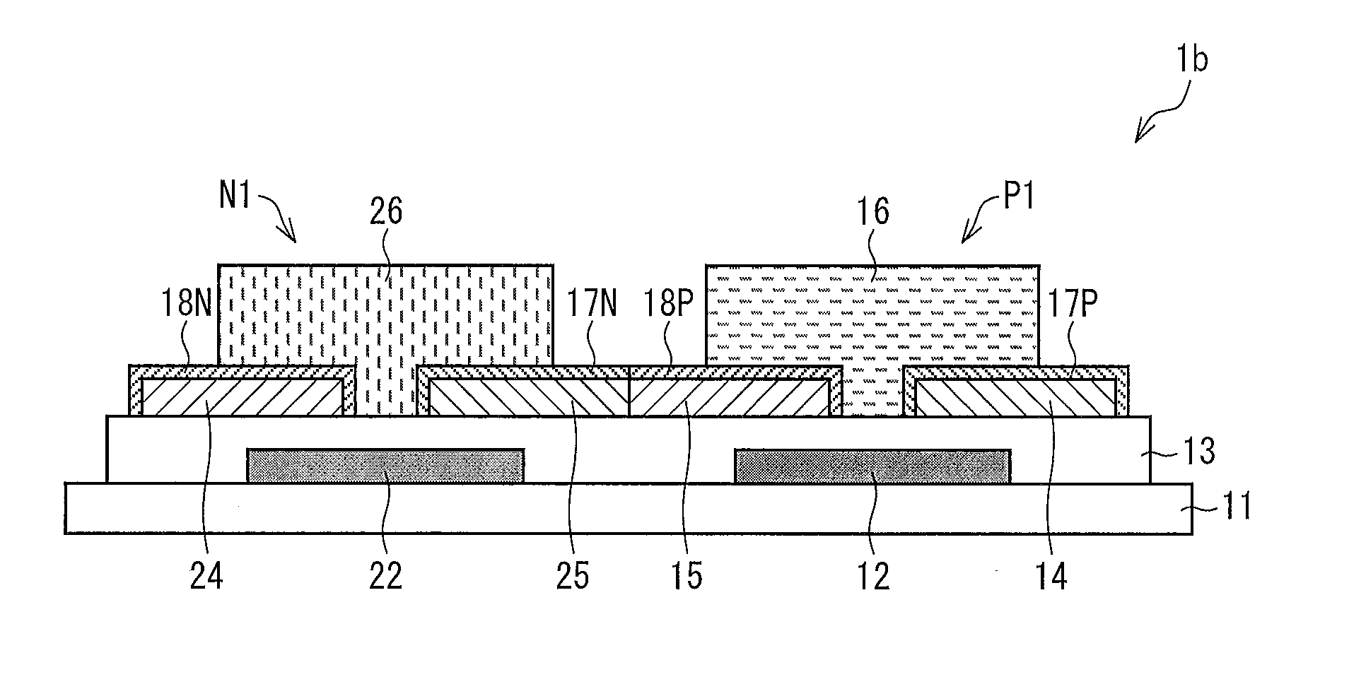
[0145]FIG. 8 is a cross-sectional view illustrating a schematic configuration of a semiconductor device of the present embodiment. As illustrated in FIG. 8, a semiconductor device 1b includes an n-type transistor N1 and a p-type transistor P1 which are provided on a same substrate 11. The semiconductor device 1b is different from the semiconductor device 1a of embodiment 1 in that the positions where the n-type transistor N1 and the p-type transistor P1 are reversed.

[0146]The semiconductor device 1b has a configuration in which a drain electrode 15 of the p-type transistor P1 and a drain electrode 25 of the n-type transistor N1 are ...

embodiment 3

[0167]The following description will discuss, with reference to FIGS. 15 and 16, still another embodiment of the semiconductor device in accordance with the present invention. For convenience, the same reference signs will be given to members having the respective same functions as those used in Embodiments 1 and 2, and descriptions on such members will be omitted.

[0168](a) of FIG. 15 is a cross-sectional view illustrating a schematic configuration of a semiconductor device of the present embodiment. Like the semiconductor device 1a illustrated in FIG. 1, a semiconductor device 1c includes an n-type transistor N1 and a p-type transistor P1 which are provided on a same substrate 11. The semiconductor device 1c has a configuration different from that of the semiconductor device 1a in that self-assembled monolayers constituting respective first layers 17P and 17N and self-assembled monolayers constituting respective second layers 18P and 18N in the semiconductor device 1c are each cons...


PUM


Abstract

A semiconductor device (1a) which is constituted by organic semiconductors with excellent transistor characteristics and includes: a p-type organic transistor (P1) having a gate electrode (12), a source electrode (14), a drain electrode (15), and a p-type organic semiconductor layer (16); an n-type organic transistor (N1) electrically connected with the p-type organic transistor (P1) and having a gate electrode (22), a source electrode (24), a drain electrode (25), and an n-type organic semiconductor layer (26); first layers for enhancing electric charge transfer, one of the first layers being provided between the source electrode (14) and the organic semiconductor layer (16), the other of the first layers being provided between the drain electrode (25) and the organic semiconductor (26); and second layers for enhancing electric charge transfer and made from a different material from that of the first layers, one of the second layers being provided between the drain electrode (15) and the organic semiconductor layer (16), the other of the second layers being provided between the source electrode (24) and the organic semiconductor layer (26), all of the source electrodes and the drain electrodes being made from a same electrode material.

Description

TECHNICAL FIELD[0001]The present invention relates to a semiconductor device and a method for fabricating the semiconductor device. Specifically, the present invention relates to (i) a semiconductor device employing a plurality of field-effect transistors each having a semiconductor layer made from organic molecules and (ii) a method for fabricating the semiconductor device.BACKGROUND ART[0002]In recent years, an organic transistor, in which an organic semiconductor material is used as an active layer, has been much attracting attention. In the organic transistor, it is possible to fabricate a device without carrying out a vacuum process and a high-temperature process at 200° C. or above, unlike in a transistor using an inorganic semiconductor such as silicon. It is also possible in the organic transistor to fabricate a device by (i) a printing technique such as an ink-jet method and a screen printing method and (ii) a solution process such as a spin coat method and a casting method...

Claims


Application Information

Patent Timeline
IPC IPC(8): H01L29/786H01L21/20
CPCH01L27/283H01L51/105H01L51/0545H10K19/10H10K10/84H10K10/466
Inventor KAMURA, MASAKAZUAOMORI, SHIGERUKUZUMOTO, YASUTAKA
Owner SHARP KK
Why Eureka
Try Eureka