Using backside passive elements for multilevel 3D wafers alignment applications

a passive element and alignment technology, applied in semiconductor/solid-state device testing/measurement, semiconductor device details, semiconductor/solid-state device testing/measurement, etc., can solve the problems of significant integration challenges of manufactures of different semiconductor technologies, and achieve the effect of improving density and performan

Active Publication Date: 2012-07-26
IBM CORP +1
View PDF4 Cites 60 Cited by
  • Summary
  • Abstract
  • Description
  • Claims
  • Application Information

AI Technical Summary

Benefits of technology

[0007]These vertically stacked chips formed from multiple die offer improved density and performance. The challenges to integrate traditionally incompatible processes on a single wafer are avoided by forming incompatible technologies on individual wafers and packaging them in the single package.
[0008]3D wafer alignment may be accomplished by using passive circuit elements formed on the back side of two wafers that will be joined together. In one embodiment, two wafers to be aligned and stacked are brought near each other and held a selected distance from each other. Passive circuit components on each wafer are thus held a known fixed distance from each other, thereby creating a capacitance between the passive circuit eleme

Problems solved by technology

As consumer demand increases for smaller multifunction devices, manufacturers face sig

Method used


Image

  • Using backside passive elements for multilevel 3D wafers alignment applications
  • Using backside passive elements for multilevel 3D wafers alignment applications
  • Using backside passive elements for multilevel 3D wafers alignment applications

Examples


Embodiment Construction

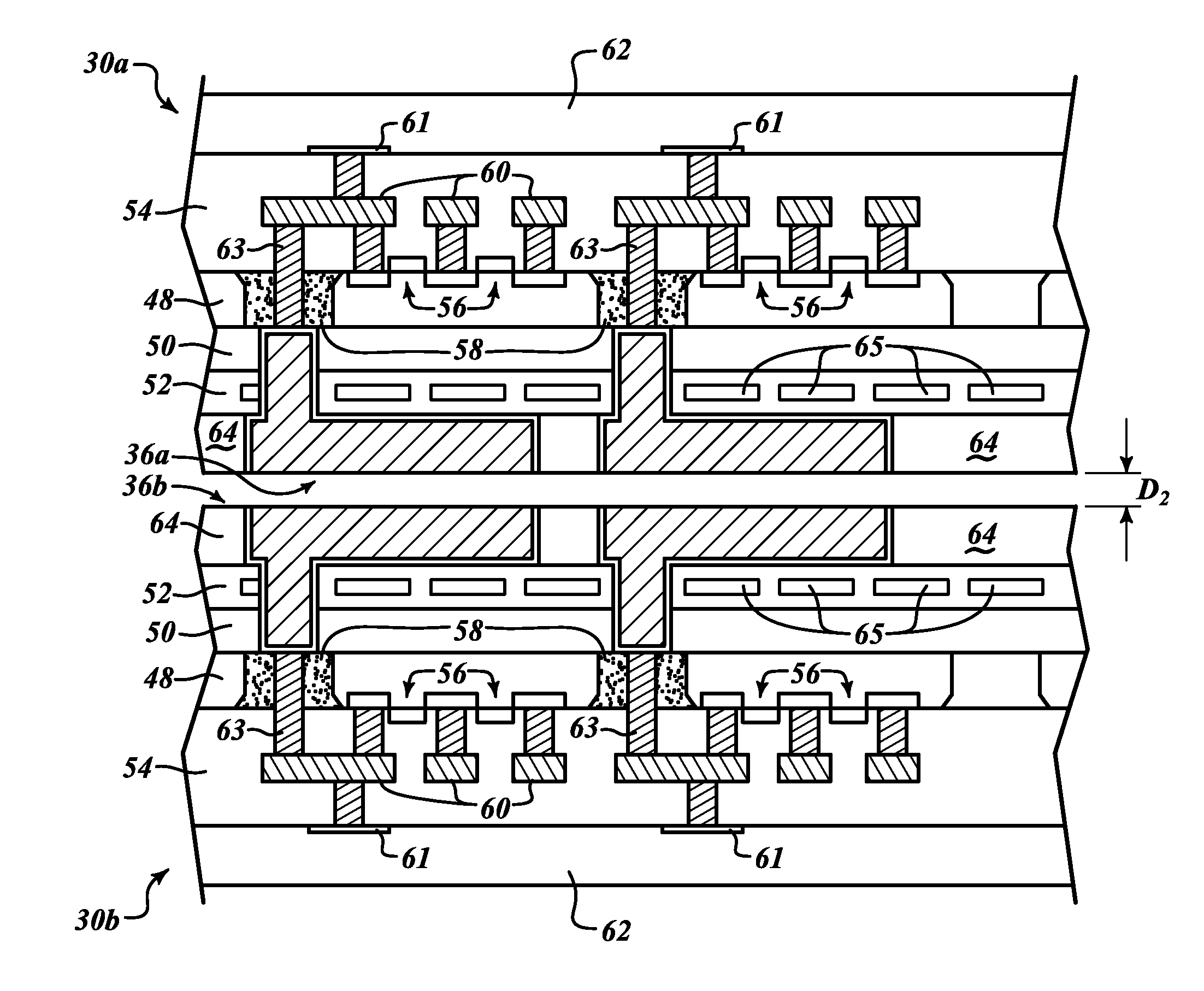
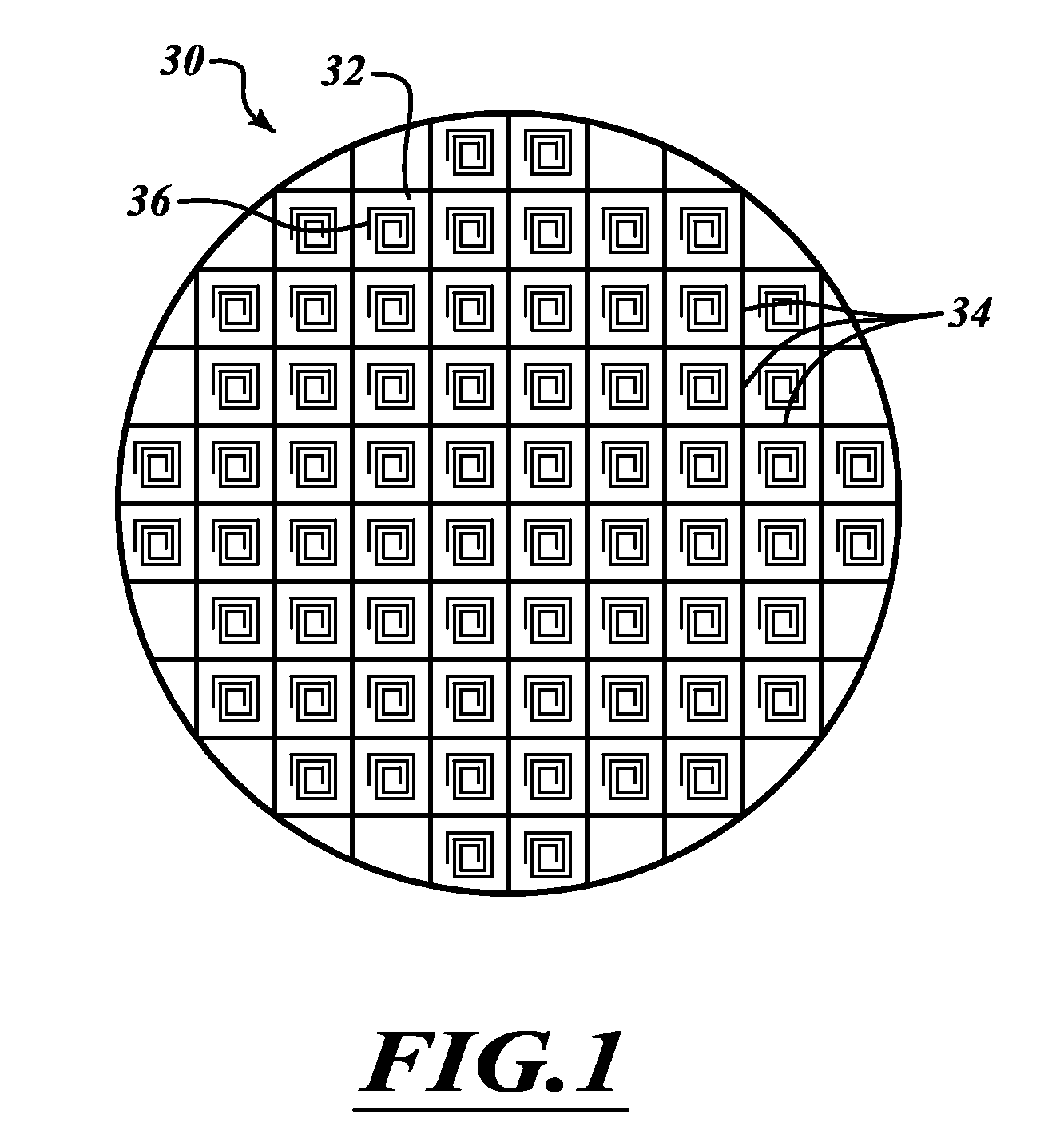
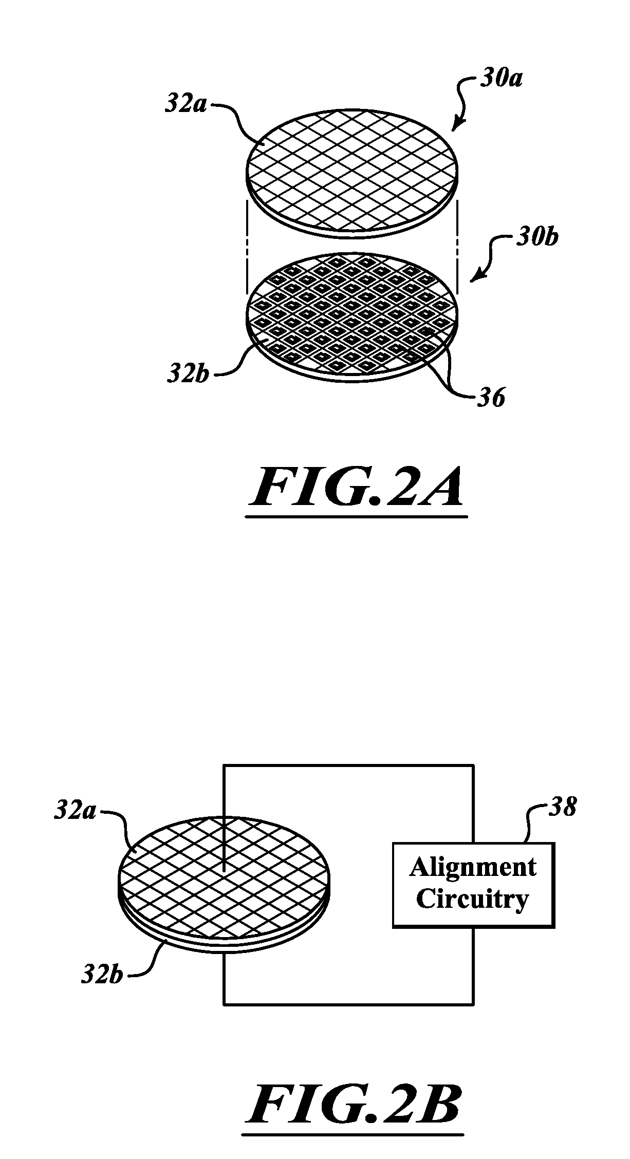
[0025]FIG. 1 is a top view of an integrated circuit wafer 30 according to one embodiment. In one embodiment, this is the back side of the wafer. The integrated circuit wafer 30 includes a plurality of individual integrated circuit dies 32. The integrated circuit dies 32 are separated from each other by scribe lines 34 in a grid pattern on the integrated circuit wafer 30. Each integrated circuit die 32 includes a passive circuit element 36 formed on or near a back surface of the integrated circuit wafer 30. Each integrated circuit die 32 includes an integrated circuit formed on a front surface of a semiconductor layer of the integrated circuit wafer 30. All of the integrated circuit dies 32 are processed simultaneously on the wafer 30.

[0026]After processing of the integrated circuit wafer 30, the integrated circuit wafer 30 will be diced into individual integrated circuit dies 32 by sawing or dicing along the scribe lines 34.

[0027]In some uses multiple integrated circuit wafers 30 ar...


PUM


Abstract

Passive circuit elements are formed at surfaces of two integrated circuit wafers. The passive circuit elements are utilized to align the two integrated circuit wafers to form an integrated circuit wafer stack.

Description

CROSS-REFERENCE TO RELATED APPLICATION[0001]This application claims the benefit under 35 U.S.C. §119(e) of U.S. Provisional Patent Application No. 61 / 436,146 filed Jan. 25, 2011 and is incorporated herein by reference in its entirety.BACKGROUND[0002]1. Technical Field[0003]The present disclosure relates to alignment structures formed on a plurality of wafers configured to be aligned to form a multichip stack in a single package.[0004]2. Description of the Related Art[0005]As consumer demand increases for smaller multifunction devices, manufacturers face significant challenges to integrate different semiconductor technologies on a single die. Multichip packages have become increasingly popular to increase device density and to combine traditionally incompatible technologies, such as logic, memory, and micro-electromechanical systems (MEMS). For example, as cell phones include more functions, such as personal entertainment systems, manufacturers look for ways to integrate multiple tec...

Claims


Application Information

Patent Timeline
IPC IPC(8): H01L27/06H01L21/66
CPCH01L24/13H01L2224/0401H01L24/80H01L24/29H01L27/0694H01L24/05H01L2924/14H01L2924/19042H01L25/50H01L2224/80805H01L2224/131H01L2224/02372H01L2224/80357H01L2924/19041H01L25/0657H01L2224/32145H01L2924/19015H01L2224/80895H01L2224/05548H01L24/94H01L24/32H01L2924/01322H01L2924/19104H01L2224/13024H01L2924/1461H01L23/645H01L2924/19043H01L2924/01029H01L2224/80896H01L2223/6677H01L2224/2919H01L2225/06541H01L2924/014H01L2924/00H01L2224/05547H01L2924/181H01L21/76898H01L23/481H01L23/5227H01L2224/80986H01L2224/80121
Inventor ZHANG, JOHN H.CLEVENGER, LAWRENCE A.XU, YIHENG
Owner IBM CORP
Why Eureka
Try Eureka