Semiconductor device and method of forming the same

a semiconductor and semiconductor technology, applied in the direction of semiconductor devices, electrical appliances, transistors, etc., can solve the problems of increasing contact resistance, difficult patterning process for forming the sti structure, and deteriorating transistor characteristics

Active Publication Date: 2012-08-23
LONGITUDE LICENSING LTD
View PDF7 Cites 34 Cited by
  • Summary
  • Abstract
  • Description
  • Claims
  • Application Information

AI Technical Summary

Benefits of technology

[0009]In still another embodiment, a semiconductor device may include, but is not limited to, a semiconductor substrate, an isolation electrode, a gate electrode, a gate insulating film, and a first insulating film. The semiconductor substrate has first and second grooves. The semiconductor substrate includes a first portion underneath the first groove and a s

Problems solved by technology

However, the patterning process for forming the STI structure has been difficult with miniaturization of the transistors.
Further, a deterioration of characteristics of th

Method used


Image

  • Semiconductor device and method of forming the same
  • Semiconductor device and method of forming the same
  • Semiconductor device and method of forming the same

Examples


first embodiment

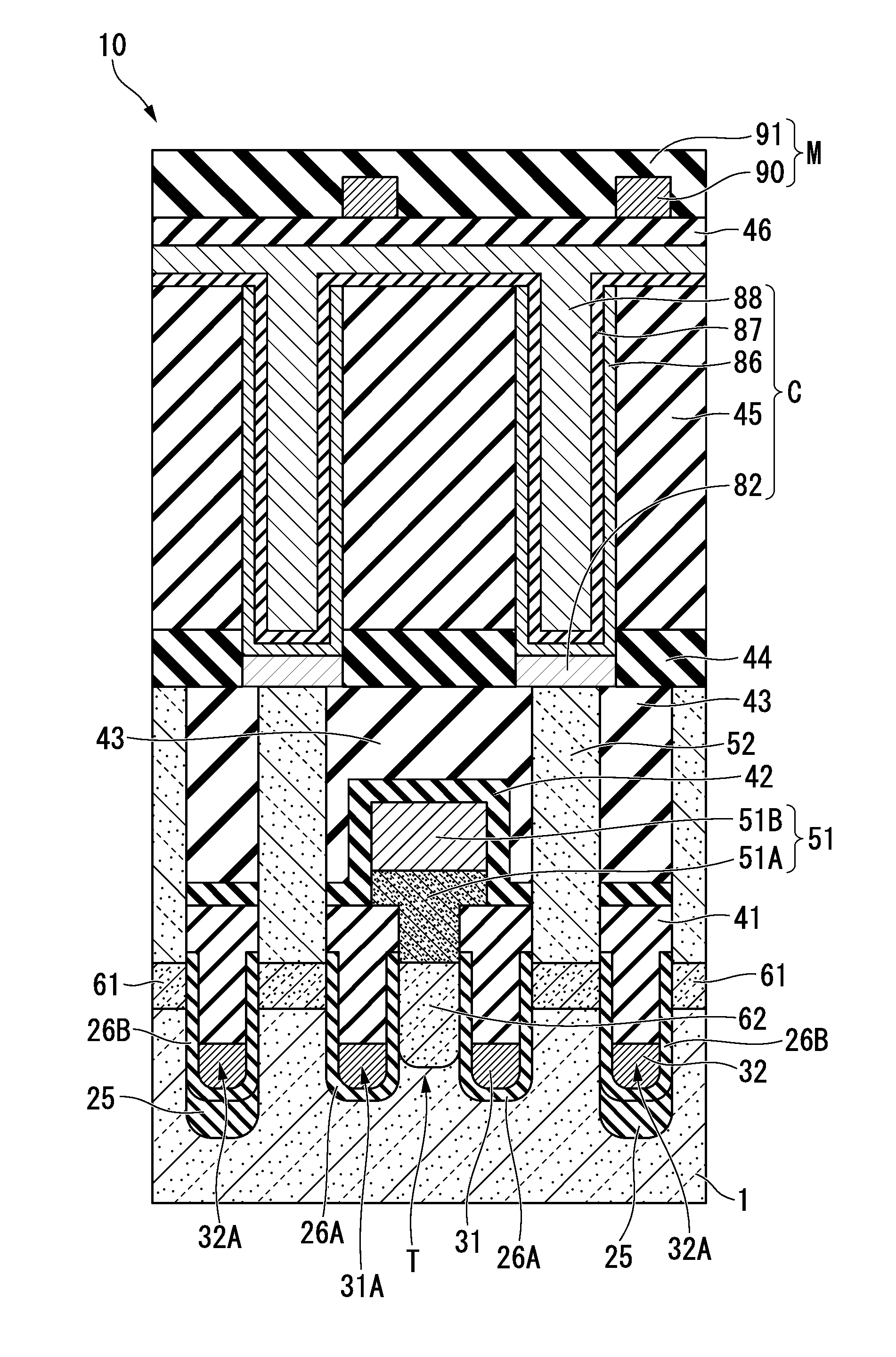
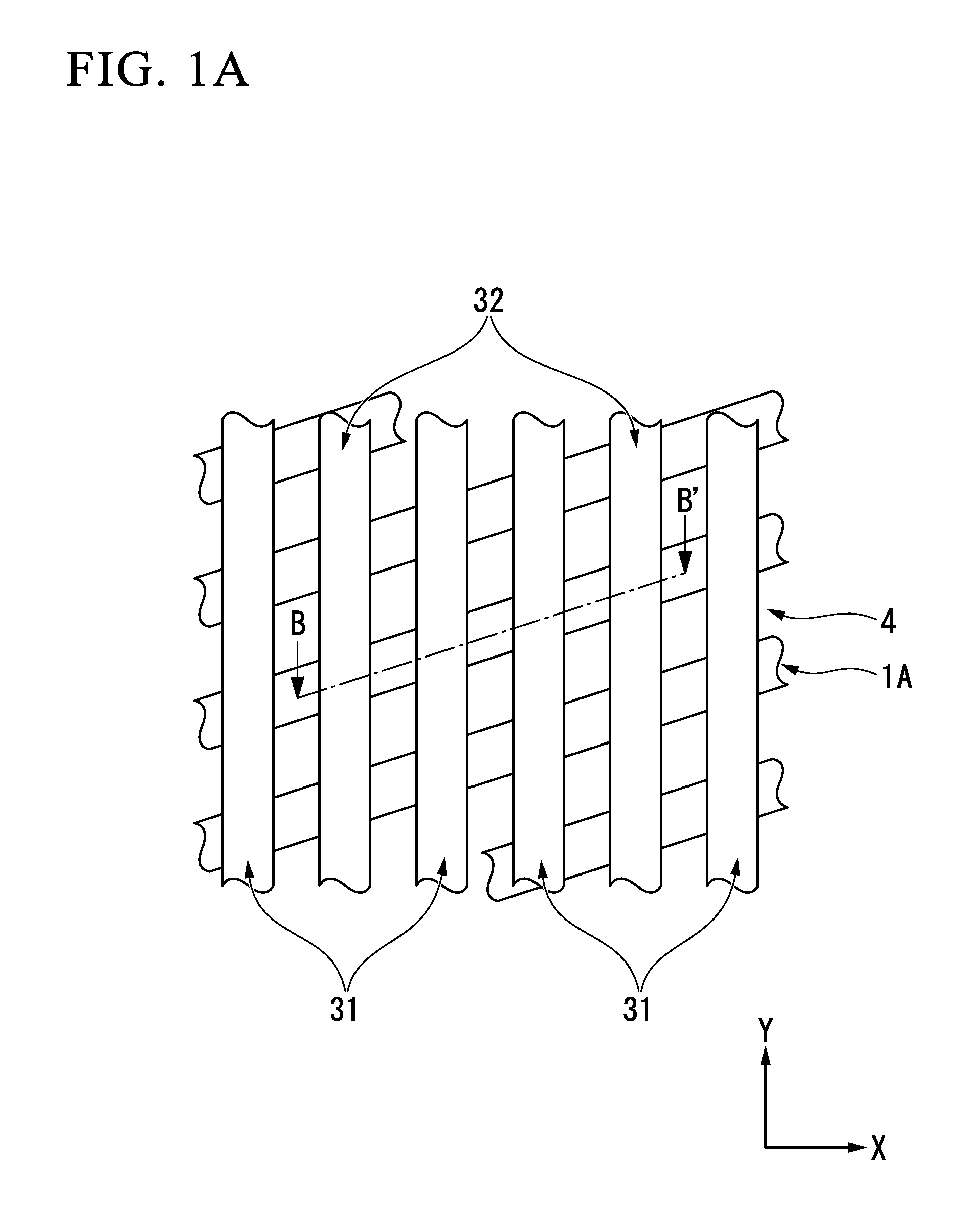
[0098]As shown in FIGS. 1A and 1B, a structure of a DRAM 10 which is obtained by applying a semiconductor device of the first embodiment will be explained. FIG. 1A is a fragmentary plan view illustrating a semiconductor device including a memory cell in accordance with a first preferred embodiment of the present invention. FIG. 1B is a fragmentary cross-sectional elevation view, taken along a B-B′ line of FIG. 1A, illustrating the semiconductor device including the memory cell in accordance with the first preferred embodiment of the present invention. In order to easily recognize parts of the semiconductor device, some elements are omitted in FIGS. 1A and 1B.

[0099]According to the present embodiment, the semiconductor device may include, but is not limited to, a plurality of active regions 1A, isolation regions 4, first isolation trenches 32A, gate trenches 31A, an insulating film 25, a gate insulating film 26A, impurity diffusion regions 61, an impurity diffusion region 62, an isol...

second embodiment

[0209]A semiconductor device according to the second embodiment will be described.

[0210]FIG. 24 is a fragmentary cross-sectional elevation view illustrating a semiconductor device including a memory cell in accordance with the second preferred embodiment of the present invention. In FIG. 24, the same parts as those in the first embodiment are denoted by the same reference numerals.

[0211]A semiconductor device 110 according to the present embodiment includes a gate electrode 131 which is a lamination electrode of an upper electrode 131B and a lower electrode 131A as shown in FIG. 24. The semiconductor device 110 includes an isolation electrode 132 which is a lamination electrode of an upper electrode 132B and a lower electrode 132A.

[0212]The upper electrode 131B includes a gate electrode material having a different work function from that of a gate electrode material included in the lower electrodes 131A. The upper electrode 132B includes a gate electrode material having a different ...

third embodiment

[0235]A semiconductor device according to the third embodiment will be described.

[0236]In order to electrically isolate the adjacent transistors, only the threshold voltage of the isolation electrode should be sufficiently higher than the threshold voltage of the gate electrodes of the adjacent transistors. A method for making the threshold voltage of the isolation electrode higher is not limited to increasing the thickness of the insulating film formed below the isolation electrode as shown in the first embodiment.

[0237]According to the present embodiment, a first impurity ion may be selectively implanted into a region 125 below the isolation electrode 32, which is a channel region, as shown in FIG. 28. A second impurity ion may be selectively implanted into a region 126 below the gate electrode 31, which is a channel region, as shown in FIG. 29.

[0238]FIG. 28 is a fragmentary cross-sectional elevation view illustrating the semiconductor device including a memory cell in accordance ...


PUM


Abstract

A semiconductor device includes a semiconductor device may include, but is not limited to, a semiconductor substrate, an isolation electrode, a gate electrode, a gate insulating film, and a first insulating film. The semiconductor substrate has a first groove and a second groove. An isolation electrode is positioned in the first groove. The gate electrode is positioned in the second groove. The gate insulating film is adjacent to the gate electrode. The first insulating film is adjacent to the isolation electrode. The isolation electrode is greater in threshold voltage than the gate electrode.

Description

BACKGROUND OF THE INVENTION[0001]1. Field of the Invention[0002]The present invention generally relates to a semiconductor device and to a method for forming a semiconductor device.[0003]Priority is claimed on Japanese Patent Application No. 2011-034896, filed Feb. 21, 2011 the content of which is incorporated herein by reference.[0004]2. Description of the Related Art[0005]Devices such as DRAMs (Dynamic Random Access Memory) in which high integration is required have necessitated miniaturization of pattern rules with miniaturization of transistors. The STI (Shallow Trench Isolation) structure is generally employed for electrically isolating adjacent transistors in a DRAM cell. However, the patterning process for forming the STI structure has been difficult with miniaturization of the transistors. Further, a deterioration of characteristics of the transistors due to the short channel effect and an increase of contact resistance due to a decrease of a contact hole diameter occur with...

Claims


Application Information

Patent Timeline
IPC IPC(8): H01L27/108
CPCH01L27/10814H01L27/10876H01L21/76224H01L27/108H01L29/7827H01L29/086H01L29/0878H01L29/4236H01L29/0653H10B12/315H10B12/053H10B12/34H10B12/00H10B12/37H01L29/0847H01L29/1025H01L29/1095H01L29/4916H01L29/4966
Inventor TAKETANI, HIROAKI
Owner LONGITUDE LICENSING LTD
Why Eureka
Try Eureka