Memory system and method of controlling same

Active Publication Date: 2012-08-30
SAMSUNG ELECTRONICS CO LTD
View PDF11 Cites 21 Cited by
  • Summary
  • Abstract
  • Description
  • Claims
  • Application Information

AI Technical Summary

Benefits of technology

[0008]These and other embodiments of the inventive concept can potentially improve reliability of semiconductor devices by reducing malfunctions

Problems solved by technology

The design of semiconductor memory systems typically involves tradeoffs.
For example, there are often tradeoffs between cost, reliability, performance, power consumption, and so on.
In a memory system having multiple semiconductor memory devices, different power management techniques can present tradeoffs between reliability and performance.
F

Method used


Image

  • Memory system and method of controlling same
  • Memory system and method of controlling same
  • Memory system and method of controlling same

Examples


Example

[0038]Embodiments of the inventive concept are described below with reference to the accompanying drawings. These embodiments are presented as teaching examples and should not be construed to limit the scope of the inventive concept.

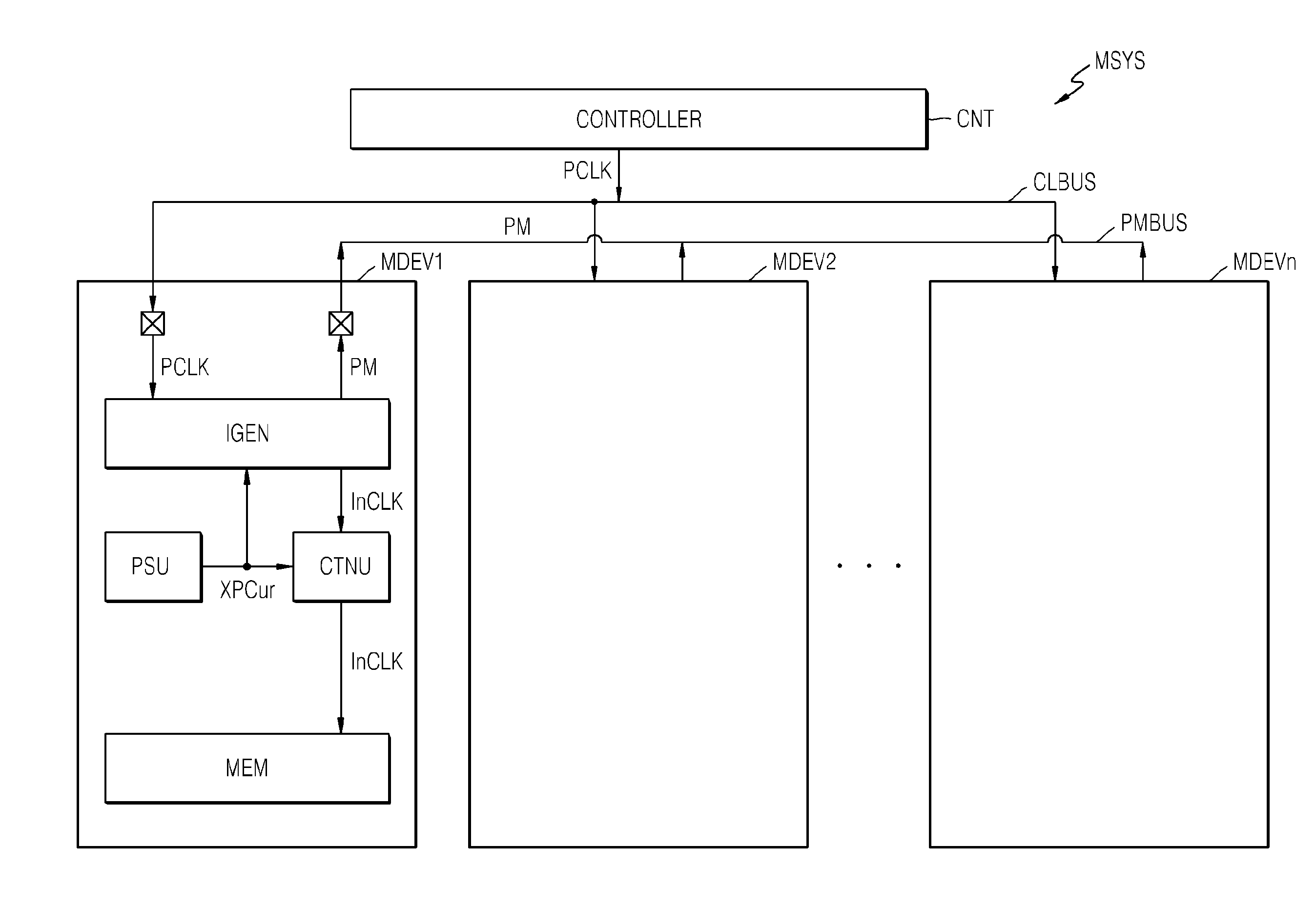
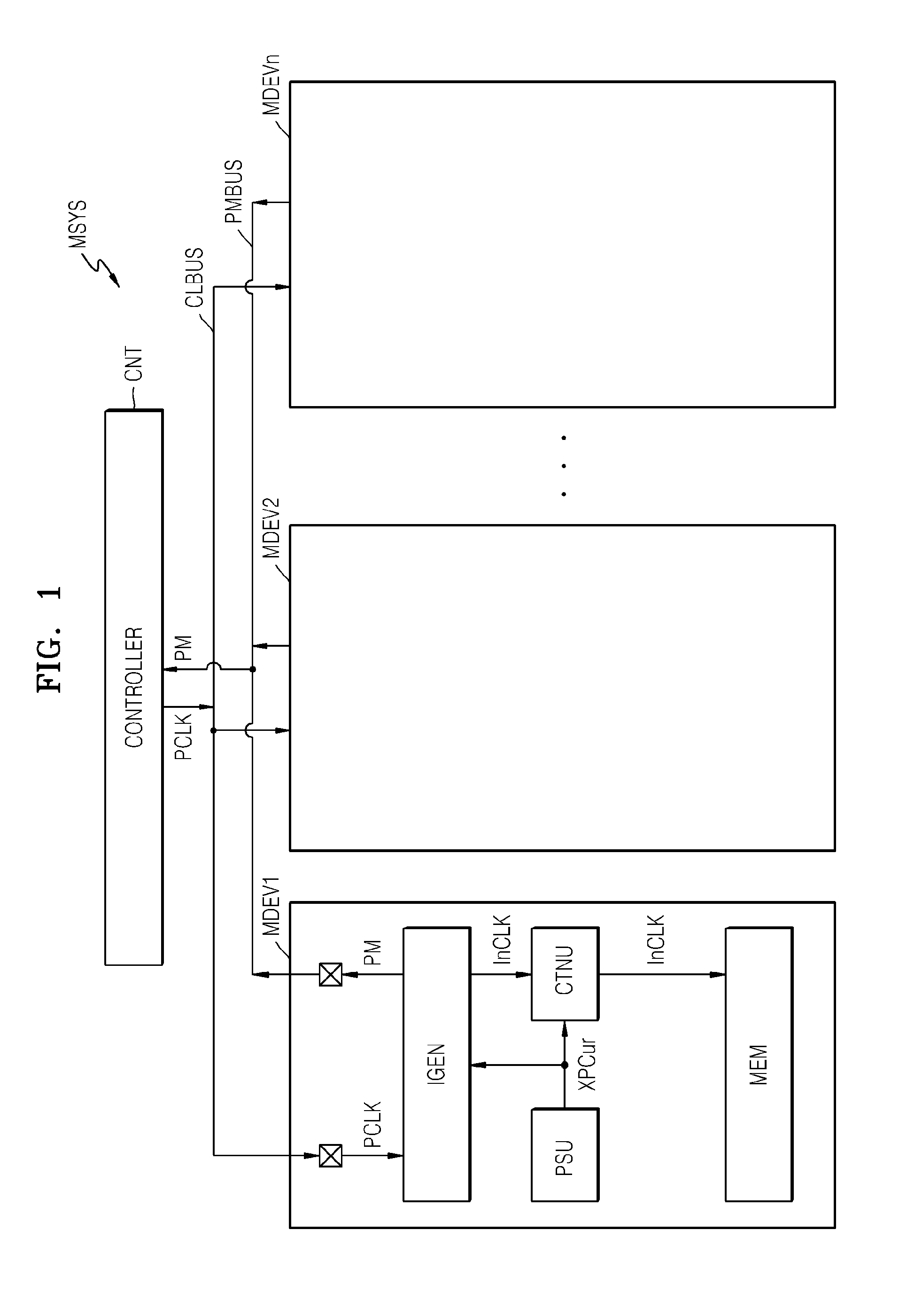
[0039]FIG. 1 is a block diagram of a memory system MSYS according to an embodiment of the inventive concept.

[0040]Referring to FIG. 1, memory system MSYS comprises a controller CNT and first through n-th memory devices MDEV1 through MDEVn. Controller CNT and first through n-th memory devices MDEV1 through MDEVn are connected to each other via a processor clock bus CLBUS and a peak signal bus PMBUS. First through n-th memory devices MDEV1 through MDEVn can be NAND flash memory devices or various other types of memory devices. The number of memory devices “n” in memory system MSYS is an integer greater than or equal to 2. Also, memory system MSYS may further comprise command and / or data buses for performing command and / or data communication between control...


PUM


Abstract

A memory system comprises a controller that generates a processor clock, and a plurality of memory devices each comprising an internal clock generator that generates an internal clock in synchronization with the processor clock, and a memory that performs a peak current generation operation in synchronization with the internal clock, wherein at least two of the memory devices generate their respective internal clocks at different times such that the corresponding peak current generation operations are performed at different times.

Description

CROSS-REFERENCE TO RELATED APPLICATIONS[0001]This application claims priority under 35 U.S.C. §119 to Korean Patent Application No. 10-2011-0017293 filed on Feb. 25, 2011 and Korean Patent Application No. 10-2011-0063039 filed on Jun. 28, 2011, the respective disclosures of which are hereby incorporated by reference.BACKGROUND OF THE INVENTION[0002]The inventive concept relates generally to electronic data storage technologies. More particularly, the inventive concept relates to semiconductor memory systems and related methods of operation.[0003]The design of semiconductor memory systems typically involves tradeoffs. For example, there are often tradeoffs between cost, reliability, performance, power consumption, and so on.[0004]In a memory system having multiple semiconductor memory devices, different power management techniques can present tradeoffs between reliability and performance. For example, in such a system, the peak currents of different memory devices may overlap, which ...

Claims


Application Information

Patent Timeline
IPC IPC(8): G06F1/12
CPCG06F1/3225Y02B60/1228G11C7/222G06F1/3275G06F13/1689Y02D10/00G06F1/14G06F1/3203G06F1/04G06F1/12G06F3/0604G06F3/0629G06F3/0683
Inventor KIM, BO-GEUNKYUNG, KYE-HYUNJEONG, JAE-YONGCHOI, SEUNG-HUNKWON, SEOK-CHEONLEE, CHUL-HO
Owner SAMSUNG ELECTRONICS CO LTD
Why Eureka
Try Eureka