Display Device

a display device and electroluminescent technology, applied in semiconductor devices, diodes, electrical apparatuses, etc., can solve the problems of increasing power consumption, loss of light, and inability to effectively use light emitted from light-emitting elements, and achieve low power consumption and high color reproducibility.

Active Publication Date: 2012-09-06
SEMICON ENERGY LAB CO LTD
View PDF2 Cites 57 Cited by
  • Summary
  • Abstract
  • Description
  • Claims
  • Application Information

AI Technical Summary

Benefits of technology

[0017]In accordance with one embodiment of the present invention, a display device that achieves low power consumption can be provided.
[0018]Further, in accordance with one embodiment of the present inven

Problems solved by technology

However, when a color filter is used, light other than light in a particular wavelength band is absorbed by the color filter, so that there is a loss of light and light emitted from a light-emitting element cannot be used effectively

Method used


Image

  • Display Device
  • Display Device
  • Display Device

Examples


embodiment 1

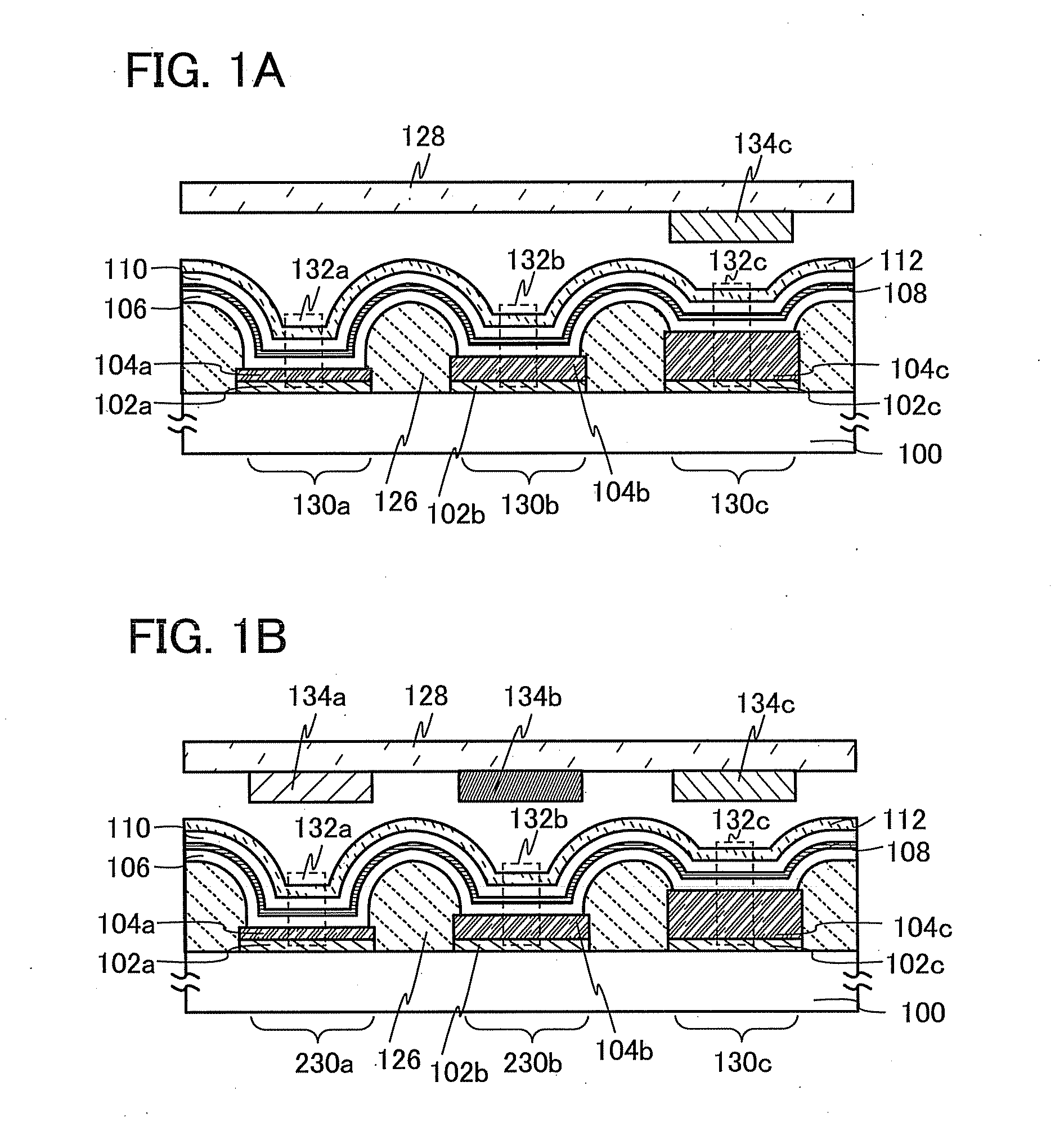
[0035]A display device in this embodiment includes a first substrate that is provided with a first light-emitting element, a second light-emitting element, and a third light-emitting element; a first region (included in a first pixel) overlapping with the first light-emitting element and sandwiched between the first light-emitting element and a second substrate; a second region (included in a second pixel) overlapping with the second light-emitting element and sandwiched between the second light-emitting element and the second substrate; a third region (included in a third pixel) overlapping with the third light-emitting element and sandwiched between the third light-emitting element and the second substrate; and a second substrate that is provided with a color filter layer in at least the third region.

[0036]The first light-emitting element includes, between a first reflective electrode and a light-transmitting electrode, a first light-emitting layer having a maximum emission peak i...

embodiment 2

[0167]In this embodiment, an active matrix display device that is one embodiment of the present invention will be described with reference to FIGS. 4A and 4B. FIG. 4A is a plan view illustrating a display device. FIG. 4B is a cross-sectional view taken along the lines A-B and C-D in FIG. 4A

[0168]In the display device illustrated in FIGS. 4A and 4B, an element substrate 410 and a sealing substrate 404 are attached to each other with a sealant 405, and a driver circuit portion (a source side driver circuit 401 and a gate side driver circuit 403) and a pixel portion 402 including a plurality of pixels are provided.

[0169]Note that a wiring 408 is a wiring for transmitting signals that are to be inputted to the source side driver circuit 401 and the gate side driver circuit 403, and receives a video signal, a clock signal, a start signal, a reset signal, and the like from a flexible printed circuit (FPC) 409 which serves as an external input terminal. Although only the FPC is illustrated...

embodiment 3

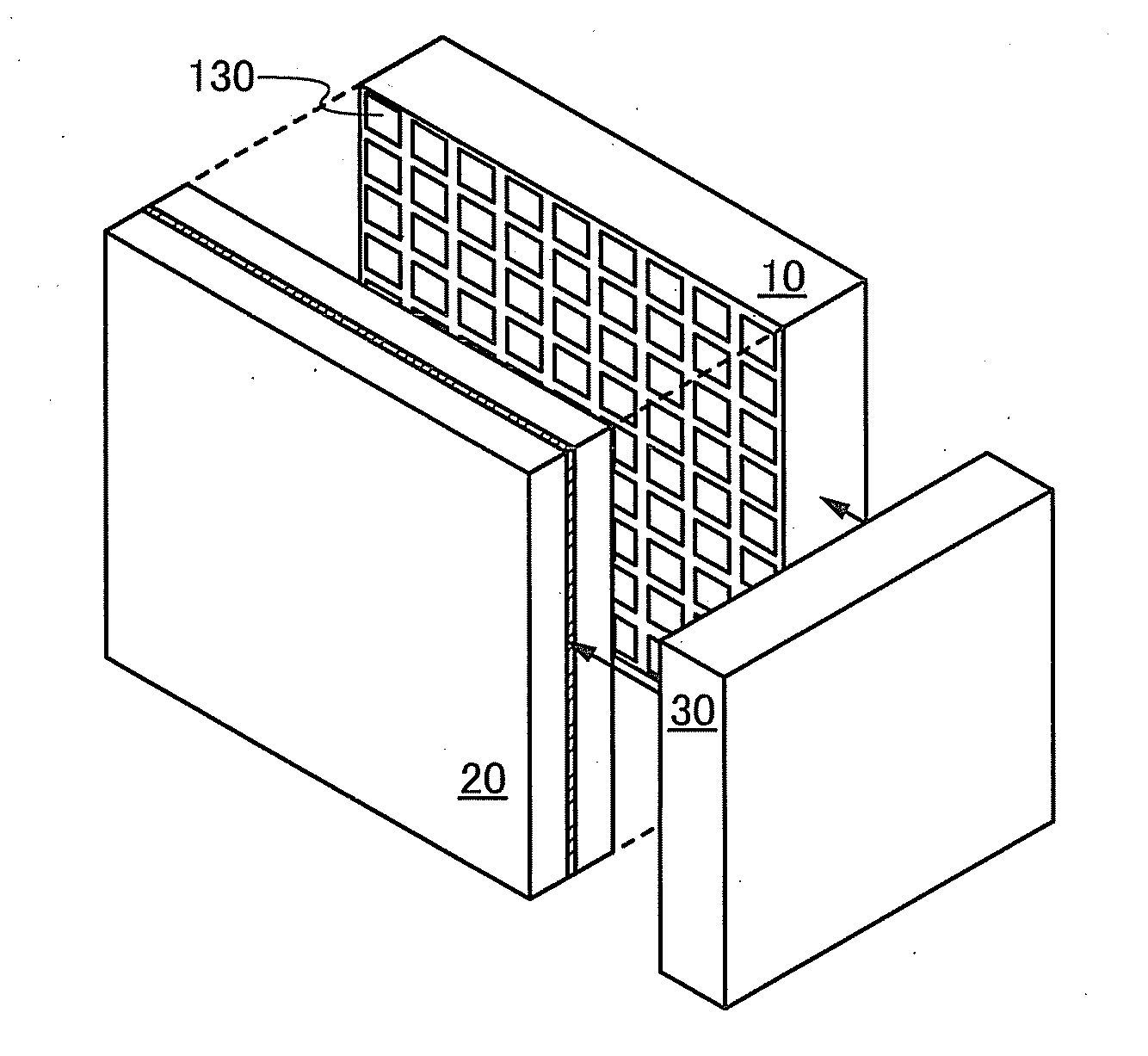
[0203]In this embodiment, a display device that is capable of three-dimensional (3D) image display and uses the display device in any of the above-described embodiments as its display panel will be described with reference to drawings.

[0204]A display device illustrated in FIG. 5A includes a display panel 10 and a shutter panel 20 that is provided on the side where light is emitted from the display panel 10, that is, a side of the display device which is viewed by a user. Note that the display device shown in FIG. 5A includes the display device in accordance with any of the above-described embodiments as the display panel 10.

[0205]The shutter panel 20 includes a plurality of optical shutter regions. Each optical shutter region includes a liquid crystal element and a switching element for selecting the transmissive or non-transmissive state of the liquid crystal element. When the liquid crystal element is put in a non-transmissive state, light emitted from the display panel 10 can be ...


PUM


Abstract

To provide a display device with low power consumption. The display device includes a plurality of pixels each having a light-emitting element having a structure in which light emitted from a light-emitting layer is resonated between a reflective electrode and a light-transmitting electrode, wherein no color filter layers are provided or color filter layers with high transmittance are provided in pixels for light with relatively short wavelengths (e.g., pixels for blue and/or green), and a color filter layer is selectively provided in pixels for light with a long wavelength (e.g., pixels for red), and thereby maintaining color reproducibility and consuming less power.

Description

BACKGROUND OF THE INVENTION[0001]1. Field of the Invention[0002]One embodiment of the present invention relates to an electroluminescence display device and a manufacturing method of the display device.[0003]2. Description of the Related Art[0004]In recent years, as display devices (so-called flat panel displays) which are very thin and light, electroluminescence (hereinafter, also referred to as EL) display devices have been attracting attentions.[0005]As a multicolor display method of an EL display device, there is proposed a method in which a light-emitting element for white light and a color filter are combined (see, for example, Patent Document 1). In this method, it has been thought that it is not necessary to separately form light-emitting elements using light-emitting materials for different emission colors in every pixel, and thus high definition can be achieved.[0006]However, when a color filter is used, light other than light in a particular wavelength band is absorbed by...

Claims


Application Information

Patent Timeline
IPC IPC(8): H01L33/08
CPCH01L27/3206H01L27/322H01L51/5265H01L51/0054H01L51/0085H01L51/006H01L51/0072H01L51/0074H01L51/0058H10K59/30H10K59/35H10K59/38H10K85/622H10K85/626H10K85/633H10K85/6576H10K85/342H10K85/6572H10K50/852H10K2102/351H10K50/11H10K50/82H10K50/818H10K2101/10
Inventor OHSAWA, NOBUHARUSASAKI, TOSHIKISEO, SATOSHI
Owner SEMICON ENERGY LAB CO LTD
Why Eureka
Try Eureka