
Solar cell and method of manufacturing the same

a solar cell and manufacturing method technology, applied in the field of solar cells, can solve the problems of high incident light reflectivity, low terminal voltage, and affecting the quality of solar cells, so as to reduce or minimize the incident light reflectivity, prevent warping of the wafer, and simplify the manufacturing process

Inactive Publication Date: 2012-09-20
SAMSUNG SDI CO LTD +1
View PDF0 Cites 4 Cited by
  • Summary
  • Abstract
  • Description
  • Claims
  • Application Information

AI Technical Summary

Benefits of technology

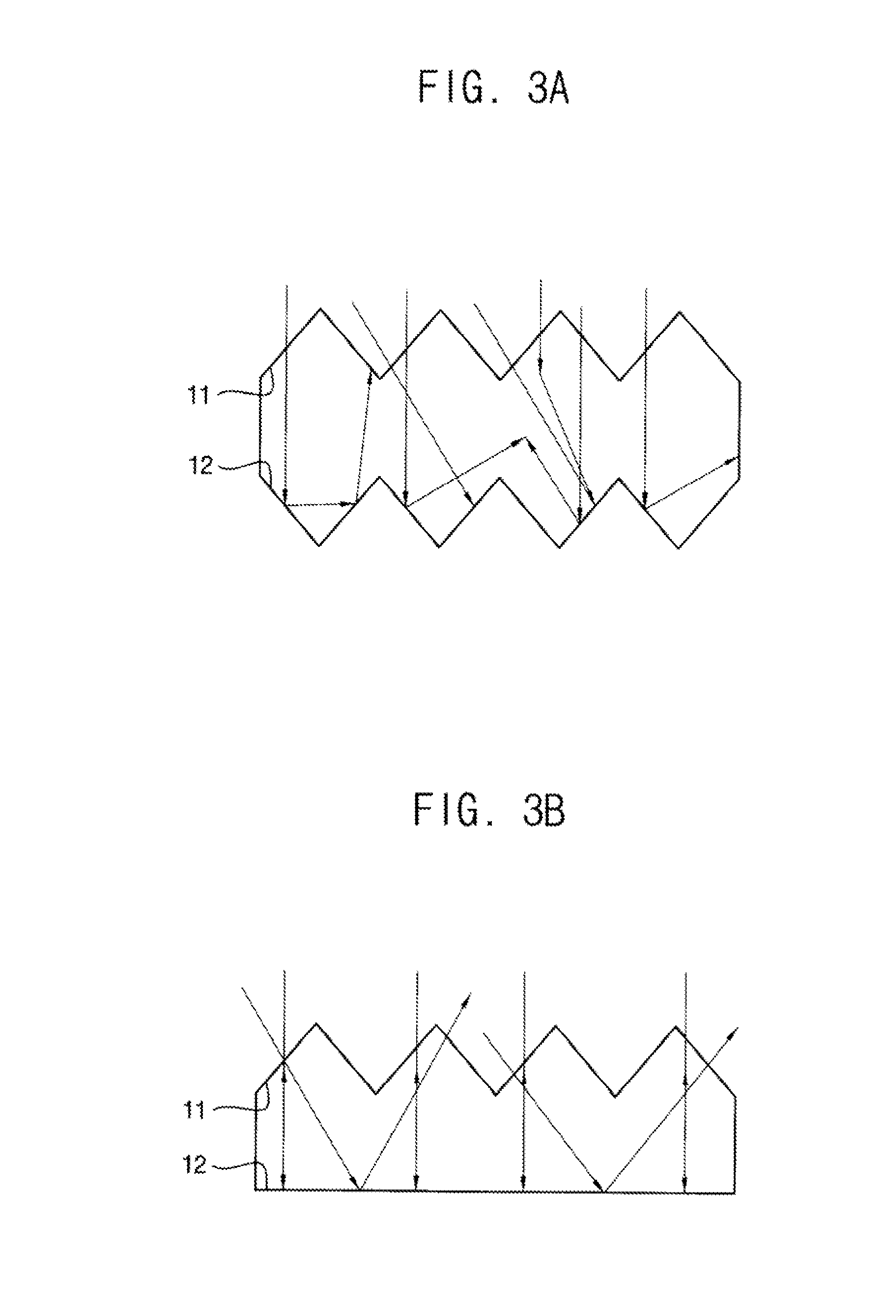
[0007]Example embodiments of the present invention provide a solar cell capable of reducing or minimizing a reflectivity of incident light, having relatively high terminal voltage, and being well-suited for a thin-film wafer.
[0023]According to the present invention, reflectivity of incident light may be reduced or minimized and a wafer including the solar cell may be kept from being bent.
[0024]In addition, a manufacturing process may be simplified, and most of the manufacturing processes may be performed at a low temperature, preventing warping of the wafer.

Problems solved by technology

Both surfaces of the hetero-junction solar cell have a pyramid shape, and thus reflectivity of incident light is high much incident light tends to be lost.
Thus, screen-printing solar cells tend to be ill-suited to thin-film wafers, and their terminal voltage tends to be relatively low.

Method used


Image

  • Solar cell and method of manufacturing the same
  • Solar cell and method of manufacturing the same
  • Solar cell and method of manufacturing the same

Examples


Embodiment Construction

[0038]Hereinafter, embodiments of the present invention will be explained in detail with reference to the accompanying drawings.

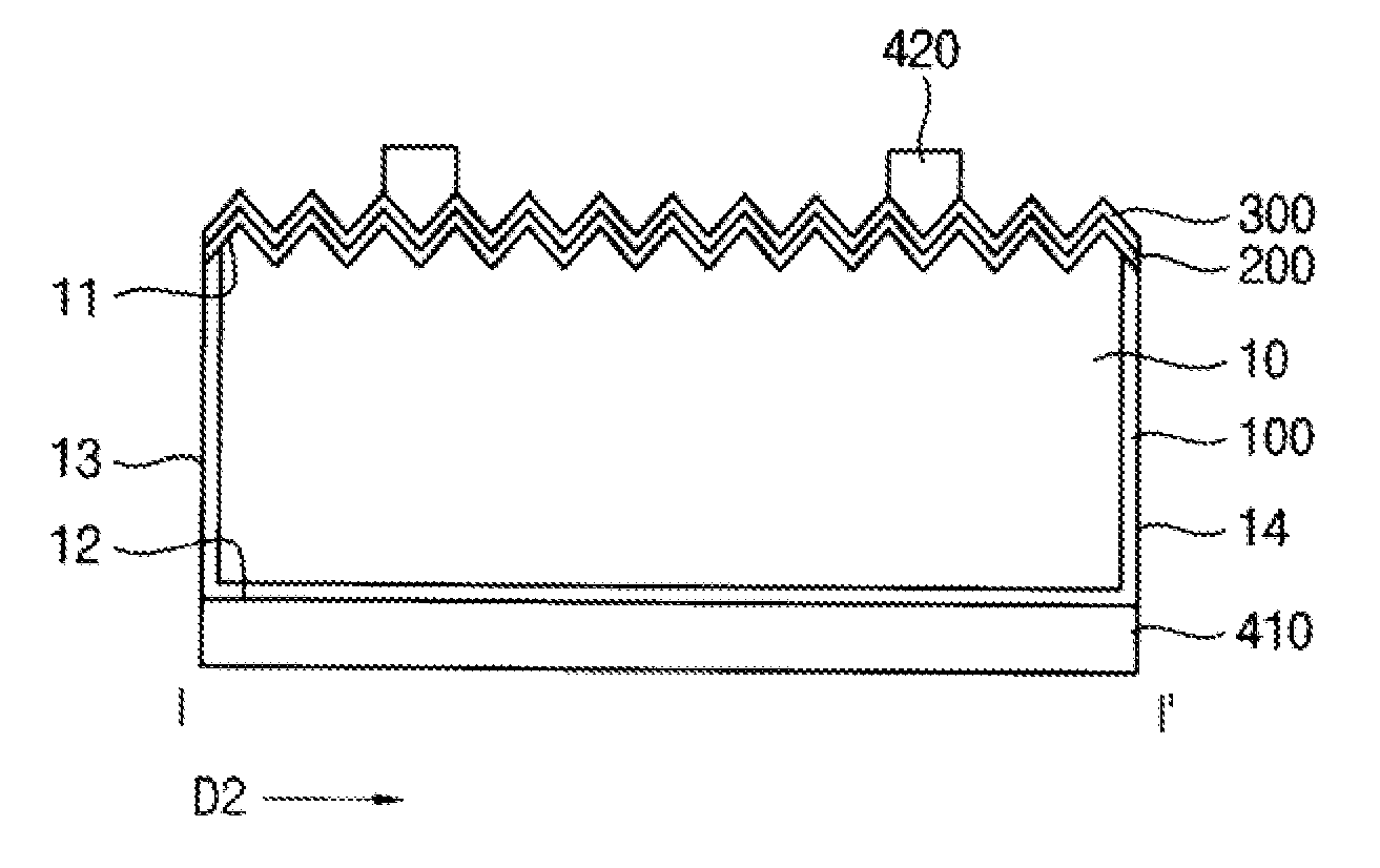
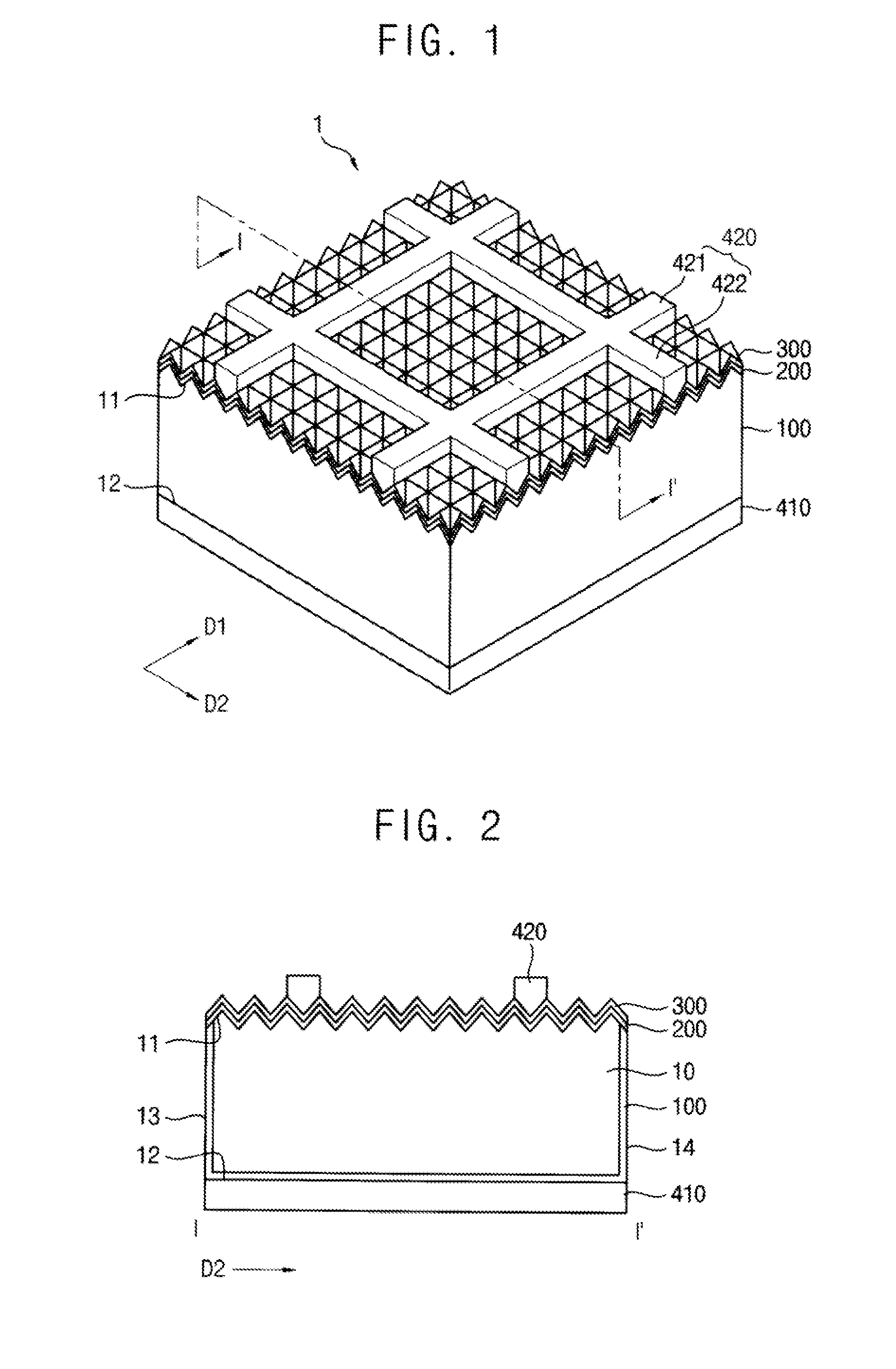
[0039]FIG. 1 is a perspective view illustrating a solar cell according to an example embodiment of the present invention. FIG. 2 is a cross-sectional view taken along a line I-I′ in FIG. 1.

[0040]Referring to FIGS. 1 and 2, the solar cell 1 according to the present example embodiment includes a base substrate 10, a first doped layer 100, a second doped layer 200, a transparent conductive layer 300, a first electrode 410 and a second electrode 420.

[0041]The base substrate 10 includes a first surface 11 into which sunlight is incident, a second surface 12 opposite to the first surface 11, a third surface 13 connecting the first surface 11 with the second surface 12, and a fourth surface 14 opposite to the third surface 13. The base substrate 10 may be an n-type crystalline silicon substrate. For example, the base substrate 10 includes an element in Group V, su...


PUM


Abstract

A solar cell and a method of manufacturing the solar cell, the solar cell including a first surface configured to receive incident sunlight and having a concavo-convex pattern, a substantially flat second surface opposite to the first surface, a first doped layer formed as a crystalline silicon layer having a first dopant, and a second doped layer formed as an amorphous silicon layer having a second dopant. The processes for forming these layers, with the exception of forming the first doped layer, are performed at a low temperature. Accordingly, reflectivity of sunlight may be minimized, a high terminal voltage may be generated, and a wafer including the solar cell can be kept from being bent.

Description

PRIORITY STATEMENT[0001]This application claims priority under 35 U.S.C. §119 to Korean Patent Application No. 2011-0024262, filed on Mar. 18, 2011, in the Korean Intellectual Property Office (KIPO), the contents of which are herein incorporated by reference in their entireties.BACKGROUND OF THE INVENTION[0002]1. Field of the Invention[0003]Embodiments of the present invention relate generally to a solar cell and a method of manufacturing the solar cell. More particularly, embodiments of the present invention relate to methods and apparatuses for making crystalline-type solar cells having higher efficiency.[0004]2. Description of the Related Art[0005]A solar cell is an energy conversion element converting light to electric energy using the photovoltaic effect. When sunlight is incident upon a substrate of the solar cell, electrons and holes are generated inside of the solar cell. The electrons and the holes respectively drift to positive and negative poles of the solar cell, so that...

Claims


Application Information

Patent Timeline
IPC IPC(8): H01L31/0232H01L31/18
CPCH01L31/02366H01L31/03682Y02E10/547Y02E10/546H01L31/1804Y02P70/50H01L31/0236H01L31/04
Inventor PARK, MINOH, MIN-SEOKLEE, YUN-SEOKSONG, NAM-KYULEE, CHO-YOUNGJEON, HOON-HAJANG, YEON-IK
Owner SAMSUNG SDI CO LTD
Learn More