Semiconductor device and method of manufacturing the same

a semiconductor device and semiconductor technology, applied in the direction of semiconductor devices, semiconductor/solid-state device details, electrical devices, etc., can solve the problems of asymmetrical behavior of the bow of the package, loss of thermal stress balance in the interior of the package, and adverse effect of the mounting of the semiconductor device, etc., to achieve the effect of suppressing the extent of the bow of the semiconductor devi

Inactive Publication Date: 2012-09-20
RENESAS ELECTRONICS CORP
View PDF6 Cites 2 Cited by
  • Summary
  • Abstract
  • Description
  • Claims
  • Application Information

AI Technical Summary

Benefits of technology

[0031]According to this semiconductor device, in a case where the center position of the first resin and the center position of the semiconductor chip deviate from each other in a direction along the surface of the wiring substrate, the center position of the semiconductor chip is caused to deviate from the center position of the wiring substrate in a direction reverse to the deviation direction of the first resin from the center position of the semiconductor chip, whereby it is possible to improve the symmetrical characteristic of a bow in the whole semiconductor device. As a result, it is possible to suppress the extent of a bow of the semiconductor device. That is, if a bow is asymmetrical, the bow warps greatly on one side, whereas making a bow symmetrical enables the amount of bow on the side where the bow is large to be reduced. Hence, it is possible to improve the mountability and mounting reliability of the semiconductor device.
[0033]According to this semiconductor device, in a case where the center position of the first resin and the center position of the semiconductor chip deviate from each other in a direction along the surface of the wiring substrate, the center position of the second resin is caused to deviate from the center position of the wiring substrate in the same direction as the deviation direction of the first resin from the center position of the semiconductor chip, whereby it is possible to improve the symmetrical characteristic of a bow in the whole semiconductor device. As a result, it is possible to suppress the extent of a bow of the semiconductor device. That is, if a bow is asymmetrical, the bow warps greatly on one side, whereas making a bow symmetrical enables the amount of bow on the side where the bow is large to be reduced. Hence, it is possible to improve the mountability and mounting reliability of the semiconductor device.
[0036]According to the present invention, it is possible to suppress the extent of a bow of a semiconductor device when the center position of the first resin and the center position of the semiconductor chip deviate from each other in a direction along one surface of the wiring substrate.

Problems solved by technology

When a semiconductor device is mounted on a wiring substrate and the temperature response of a bow at the temperature at which reflow is performed is asymmetrical, this can exert an adverse effect on the mountability of the semiconductor device.
Therefore, the thermal stress balance in the interior of the package becomes lost and the bow of the package exhibits an asymmetrical behavior.
As described above, asymmetry of the bow characteristics of a package results in a decrease in the margin of mountability, a decrease in mounting yield, and a decrease in mounting reliability.
Such adverse effects of asymmetry of bows have become manifest particularly in packages in which recent thin boards of less than 400 μm are used.
As described above, it has been difficult to suppress the extent of bows of semiconductor devices when the center of an underfill resin deviates from the center of a chip due to the asymmetry of the fillet width of the underfill resin.

Method used


Image

  • Semiconductor device and method of manufacturing the same
  • Semiconductor device and method of manufacturing the same
  • Semiconductor device and method of manufacturing the same

Examples


first embodiment

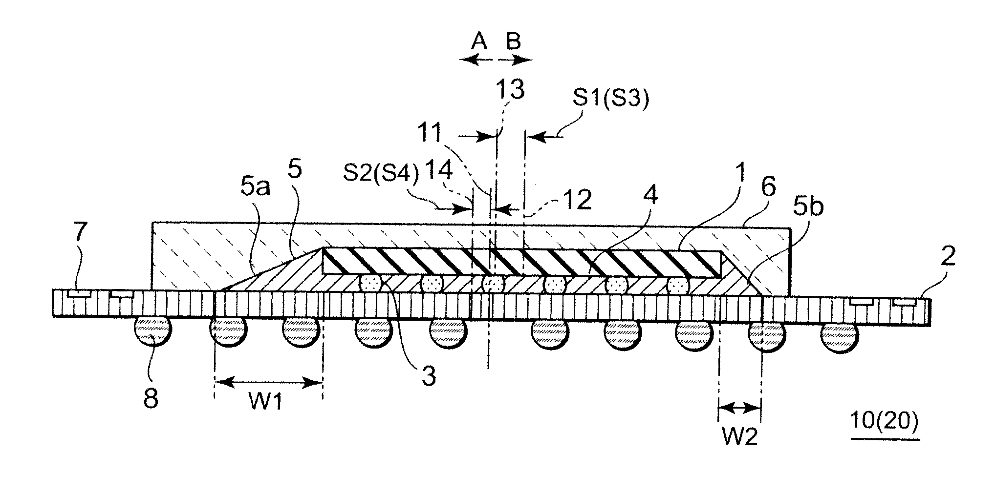
[0067]FIG. 1 is a sectional view of a semiconductor device 10 of the first embodiment.

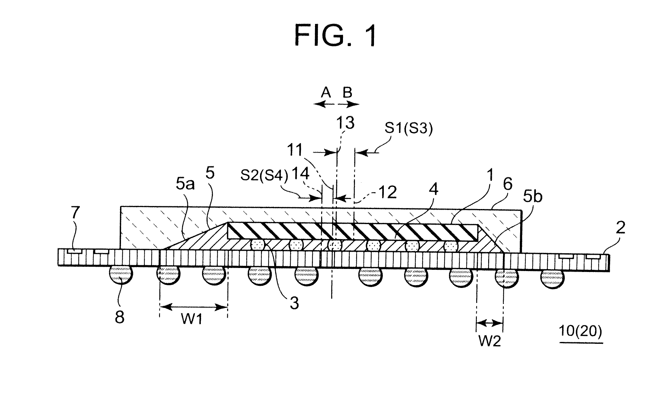
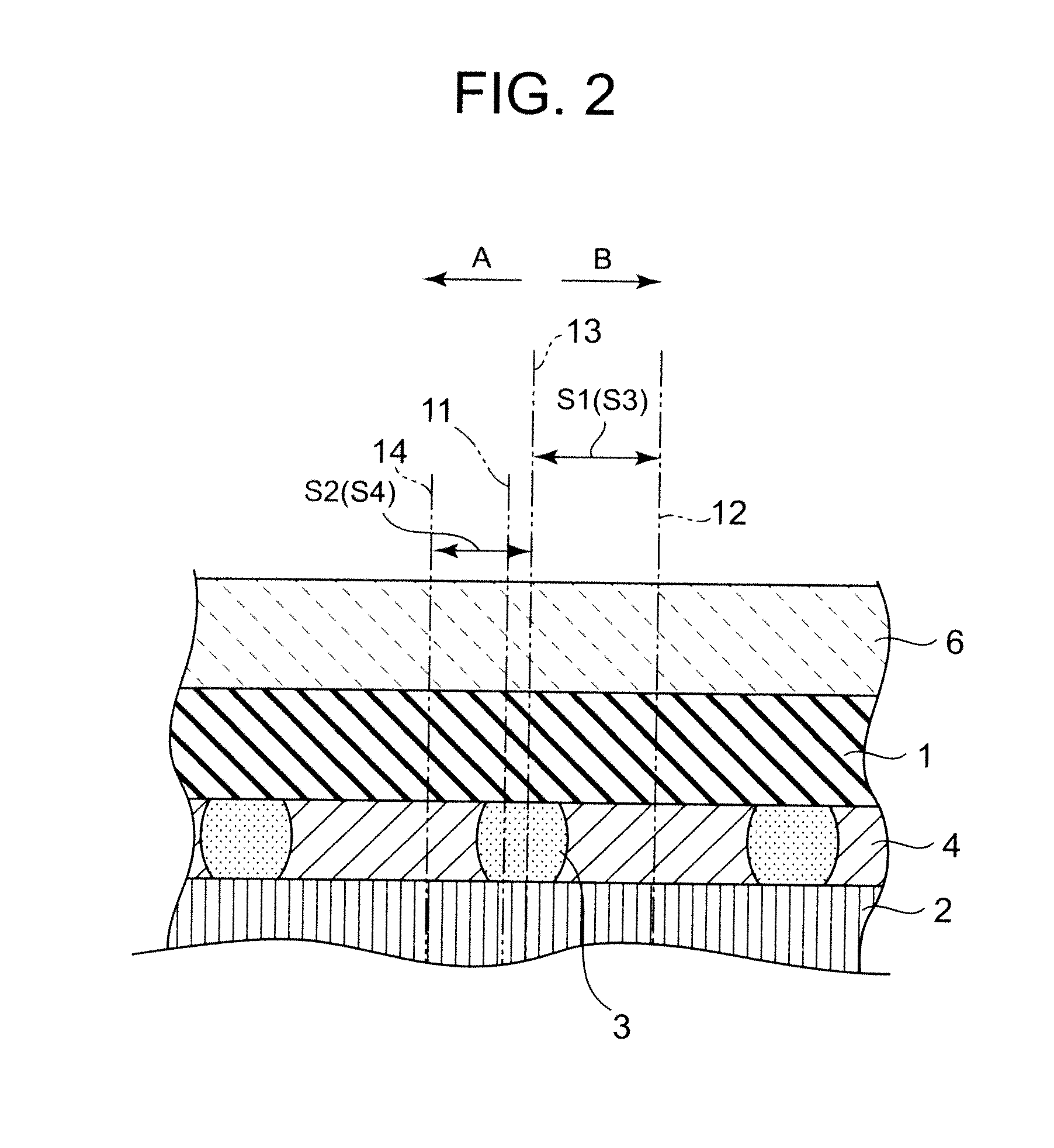
[0068]FIG. 2 is an enlarged view of an essential portion of FIG. 1. FIGS. 3 and 4 are plan views of the semiconductor device 10 of the first embodiment. FIG. 4 shows the action (a movement line 18) of an underfill resin injection nozzle (not shown) during the formation of an underfill resin 4. FIG. 5 is an enlarged view of an essential portion of FIG. 3. Incidentally, FIGS. 3 and 4 show the condition before the singulation of each semiconductor device (package) 10. FIGS. 6A to 6E are plan views showing the flow of a series of steps to explain the manufacturing method of the semiconductor device of the first embodiment.

[0069]The semiconductor device 10 of the present embodiment includes a wiring substrate 2, a semiconductor chip 1 mounted on the wiring substrate 2 in such a manner that one surface thereof is opposed to one surface of the wiring substrate 2, and a first resin (an underfill resin 4) w...

second embodiment

[0113]FIGS. 7 and 8 are plan views of the semiconductor device 20 of the second embodiment. FIG. 9 is an enlarged view of an essential portion of FIG. 7. FIG. 8 shows the action (a movement line 18) of an underfill resin injection nozzle (not shown) during the formation of an underfill resin 4. Incidentally, FIGS. 7 and 8 show the state before the singulation of each semiconductor device (package) 20. FIGS. 1 and 2, which were described in connection with the semiconductor device 10, serve also as sectional views of the semiconductor device 20.

[0114]The movement line 18 shown in FIG. 8 is a movement line of a leading end position 17 of an underfill resin injection nozzle (not shown) during the formation of the underfill resin 4 in the case of this embodiment. This embodiment is a case where, as shown in FIG. 8, the underfill resin 4 is injected into the gap between a board 2 and a semiconductor chip 1 while the underfill resin injection nozzle is being moved in a manner of the lette...

third embodiment

[0131]FIG. 10 is a sectional view of a semiconductor device 30 of the third embodiment. FIG. 11 is an enlarged view of an essential portion of FIG. 10. FIGS. 12 and 13 are plan views of the semiconductor device 30 of the third embodiment. FIG. 13 shows the action (a movement line 18) of an underfill resin injection nozzle (not shown) during the formation of an underfill resin 4. FIG. 14 is an enlarged view of an essential portion of FIG. 12. Incidentally, FIGS. 12 and 13 show the condition before the singulation of each semiconductor device (package) 30.

[0132]As is apparent from FIGS. 10 to 14, the third embodiment differs from the first embodiment only in the point that the amount of deviation S2 of the center position 14 of a resin for encapsulation 6 from the center position 13 of a board 2 is 0. In other respects, the third embodiment is the same as in the first embodiment.

[0133]According to the third embodiment, the same effect as in the first embodiment is obtained.


PUM


Abstract

A method of manufacturing a semiconductor device, includes mounting a semiconductor chip on a wiring substrate such that one surface of the semiconductor chip is faced to one surface of the wiring substrate, and filling a first resin in a gap between the surface of the wiring substrate and the surface of the semiconductor chip such that part of the first resin protrudes from the gap. In the filling of the first resin, the first resin is injected into the gap by use of a first resin injection nozzle while the first resin injection nozzle is being moved along any one of sides of the semiconductor chip or along two sides of the semiconductor chip which are adjacent to each other.

Description

[0001]The present application is a Divisional Application of U.S. patent application Ser. No. 12 / 659,766, filed on Mar. 19, 2010, which is based on Japanese patent application No. 2009-80212, filed on Mar. 27, 2009, the entire contents of which is incorporated herein by reference.BACKGROUND OF THE INVENTION[0002]1. Field of the Invention[0003]The present invention relates to a semiconductor device and a method of manufacturing the semiconductor device.[0004]2. Description of the Related Art[0005]As a small-area, thin semiconductor package (hereinafter simply called “a package”) that permits high-density packaging, there is available a package in which the flip-chip mounting method is adopted for an electrical connection between a semiconductor chip (hereinafter simply called “a chip”) and a wiring substrate (hereinafter simply called “a board”). In recent years, demand for this type of package has been increasing.[0006]FIGS. 25 and 26 are diagrams showing a general semiconductor dev...

Claims


Application Information

Patent Timeline
Patent Type & Authority Applications(United States)
IPC IPC(8): H01L21/56
CPCH01L21/563H01L2924/014H01L24/32H01L24/97H01L2224/16225H01L2224/73203H01L2224/73204H01L2224/97H01L2924/01029H01L2924/01079H01L2924/01082H01L2924/15311H01L2924/3511H01L23/3128H01L2924/01033H01L2924/01006H01L2924/01005H01L2224/32225H01L2224/81H01L2924/00012H01L2924/00H01L2924/00014H01L2924/00011H01L2224/0401
Inventor SAKATA, KENJIKIDA, TSUYOSHI
Owner RENESAS ELECTRONICS CORP
Why Eureka
Try Eureka