Thin Film Forming Method and Quantum Dot Device
- Summary
- Abstract
- Description
- Claims
- Application Information
AI Technical Summary
Benefits of technology
Problems solved by technology
Method used
Image

Examples
first embodiment
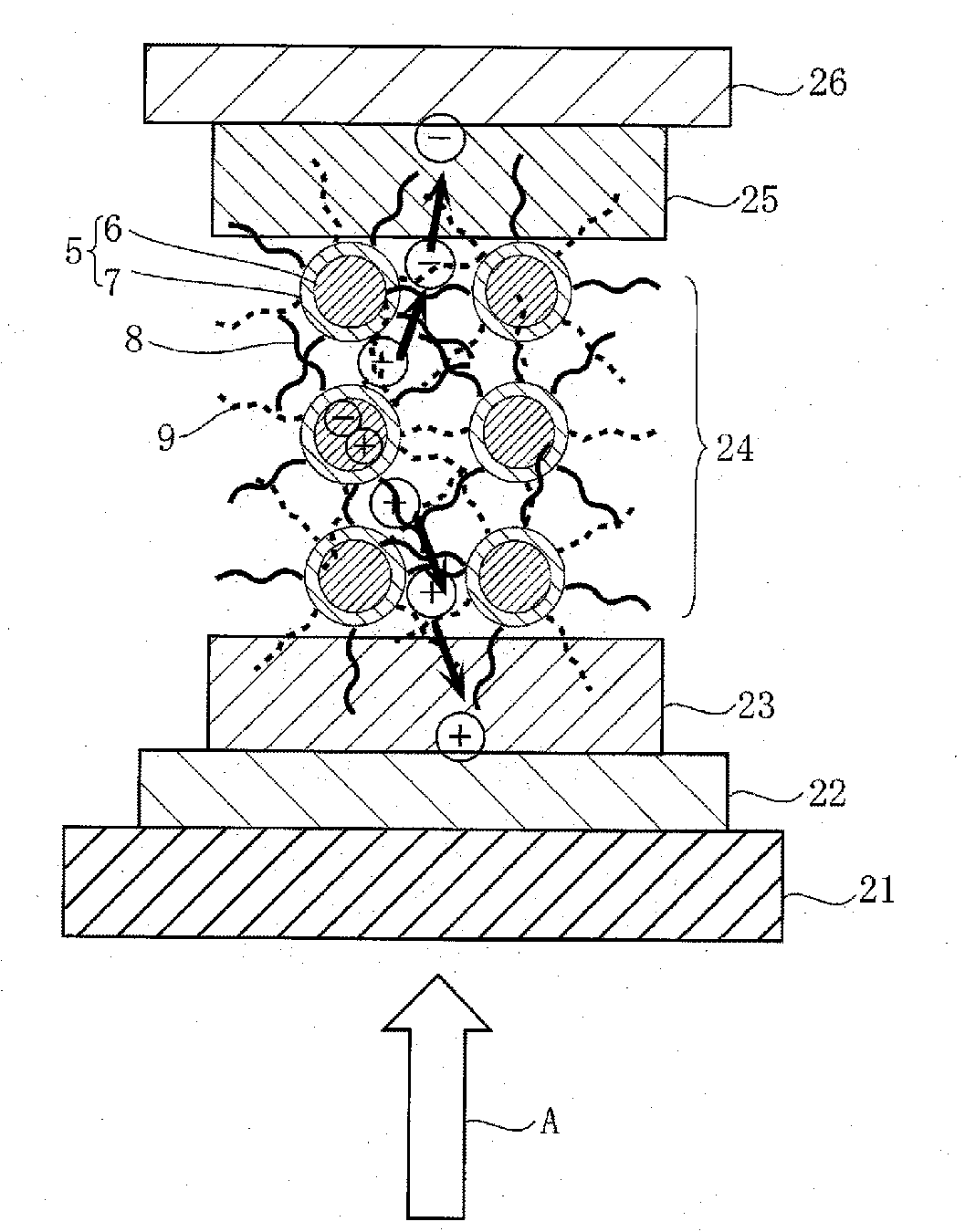
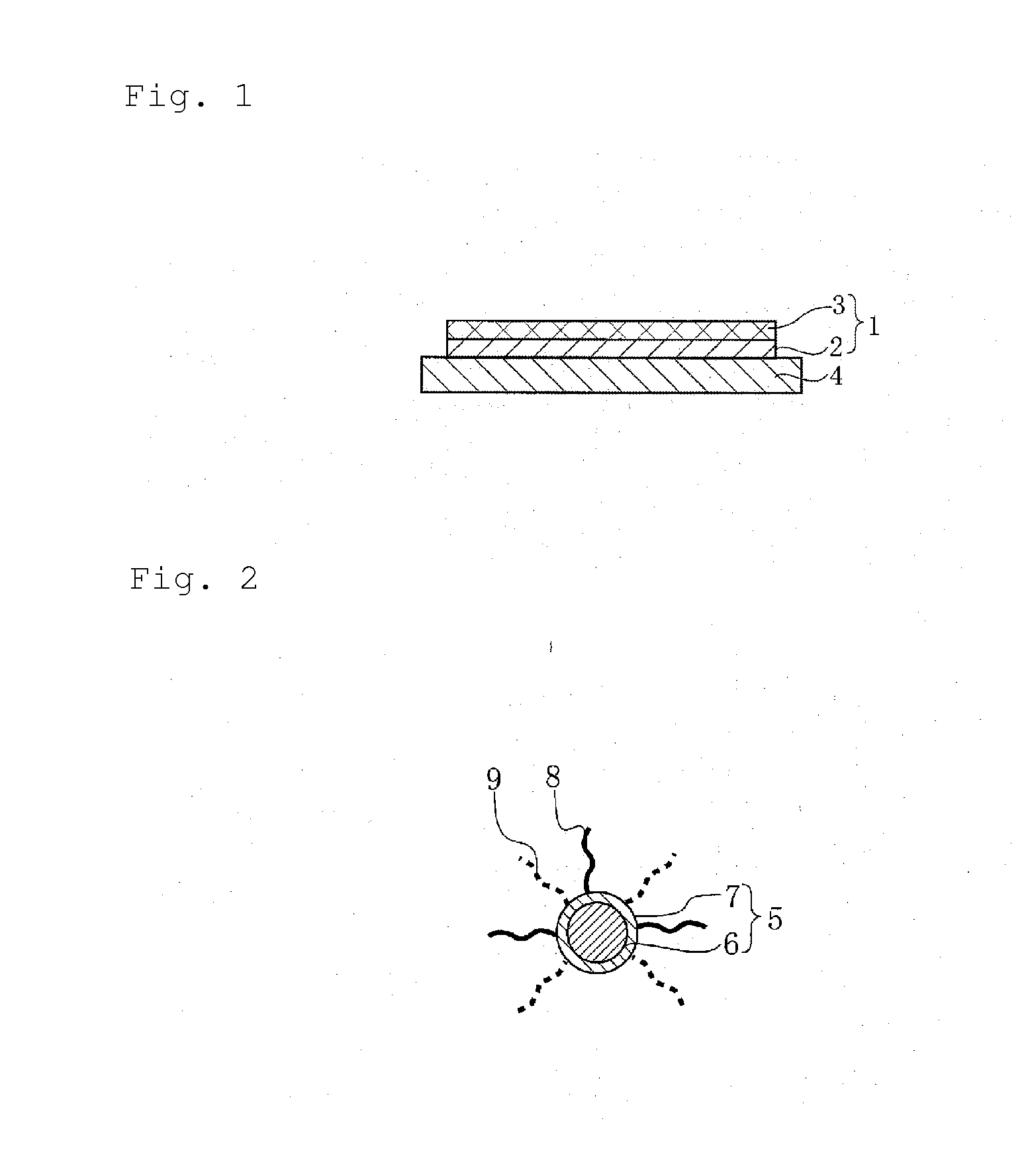
[0102]As described above, in the first embodiment, the electron transport QD dispersed solution 16 is prepared in which the electron transporting surfactant 9 is coordinated on the surfaces of the quantum dots 5, and subjected to vacuum drying, and then, the hole transporting surfactant 8 prepared in large amounts as compared with the electron transporting surfactant 9 is brought into contact with the electron transport QD 14 in the solution to prepare the hole-electron transport QD dispersed solution 20 with a portion of the electron transporting surfactant 9 replaced with the hole transporting surfactant 8. Thus, the need for a series of complicated step for removing suspended ligands is eliminated to make it possible to easily carry out the ligand replacement treatment 12c without peeling of the carrier transporting surfactants 8, 9 from the surface of the quantum dots 3. More specifically, the desired ligand replacement operation can be carried out without providing a series of ...
second embodiment
[0126]FIG. 9 is a cross-sectional view schematically illustrating a thin film prepared by the use of a thin film forming method according to the present invention.
[0127]This thin film 31 has a two-layer structure of an electron transport layer 32 containing an electron transporting surfactant (second surfactant) as its main constituent and a quantum dot layer 33, and is formed on a substrate 34.
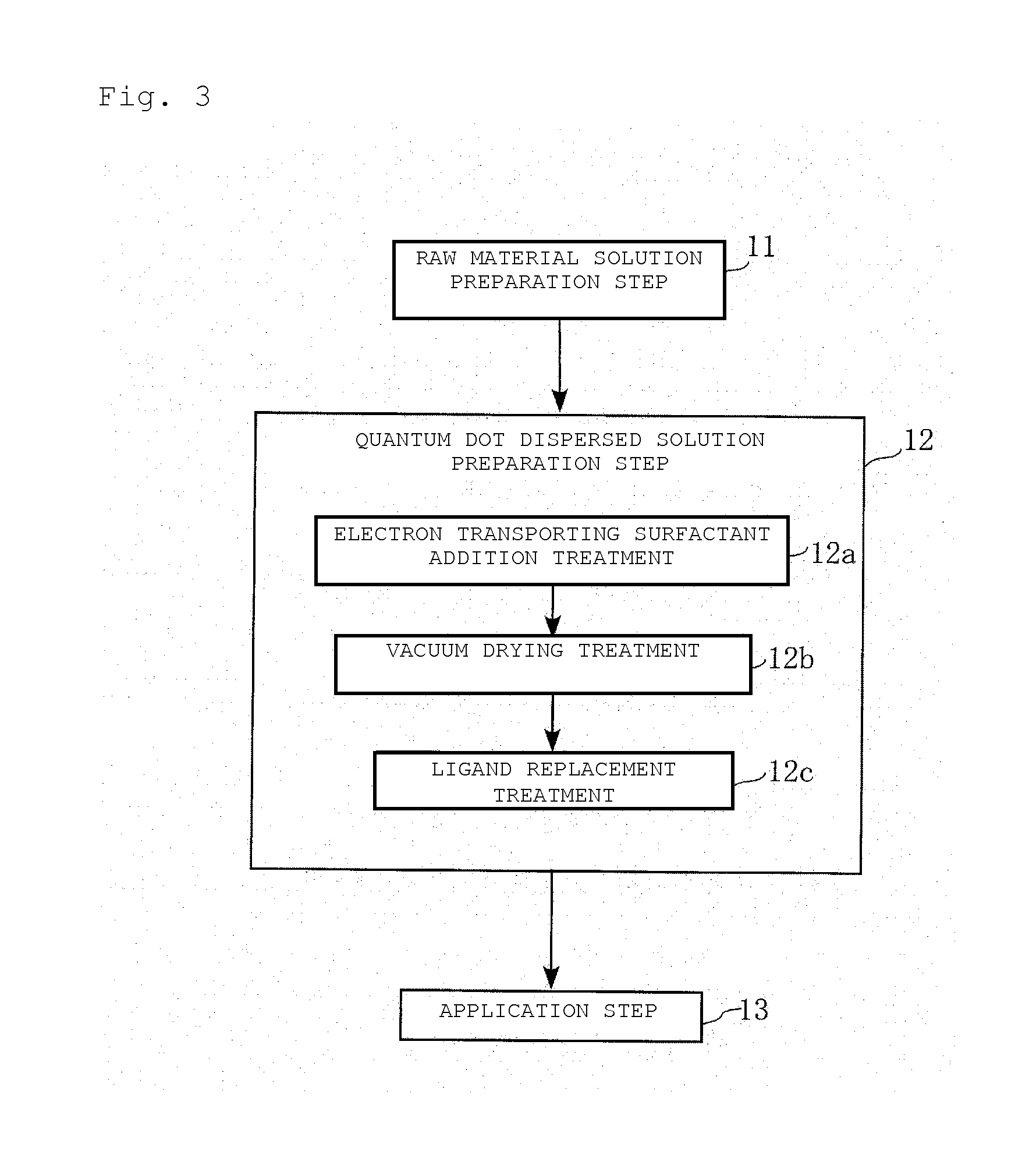
[0128]FIG. 10 is a production step diagram showing an preparation method of the thin film 31.
[0129]More specifically, in a raw material solution preparation step 35, a raw material solution such as an InP / ZnS dispersed solution is prepared in the same manner and procedure as in the first embodiment.
[0130]Then, in a quantum dot dispersed solution preparation step 36, a hole transporting surfactant addition treatment 36a is carried out. More specifically, a hole transporting surfactant 8 is added to the raw material solution to coat the surfaces of quantum dots 5 with the hole transporting surf...
third embodiment
[0143]It is to be noted that the present invention is not limited to the embodiments described above. While the large amount of the hole transporting surfactant 8 is put and thereby immersed in the electron transport QD dispersed solution in the third embodiment, it goes without saying that the same shall apply to the case where a large amount of the electron transporting surfactant 9 is put and thereby immersed in a hole transport QD dispersed solution.
[0144]In addition, while the quantum dots 5 have the core-shell structure composed of the core section 6 and the one-layer shell section 7 in the respective embodiments, the present invention can be also applied likewise to a core-shell-shell structure with the shell section 7 composed of a two-layer structure, and a quantum dot without any shell section.
[0145]In addition, as for photoelectric conversion devices for achieving the conversion from electrical signals to optical signals, the present invention can be also applied likewise...
PUM
 Abstract
Description
Claims
Application Information