Eureka AIR delivers breakthrough ideas for toughest innovation challenges, trusted by R&D personnel around the world.

Approach to intergrate schottky in mosfet

Active Publication Date: 2012-10-04
ALPHA & OMEGA SEMICON INC
View PDF0 Cites 35 Cited by
  • Summary
  • Abstract
  • Description
  • Claims
  • Application Information

AI Technical Summary

Problems solved by technology

Power MOSFETs that implement P-N junction diodes exhibit several undesirable characteristics, which include: large forward conduction loss, storage of charge between body-epitaxial junction when operating in forward bias, excess stored minority charges which cause large recovery currents and voltage overshoots when the power MOSFET is switched from forward bias to reverse bias, generation of radio frequency interference during fast switching.
All of these characteristics cause unnecessary stress to the device, leading to sub-optimal performance.
The low forward drop of the Schottky diode during forward conduction reduces power dissipation of the device and leads to lower conduction loss.

Method used


Image

  • Approach to intergrate schottky in mosfet
  • Approach to intergrate schottky in mosfet
  • Approach to intergrate schottky in mosfet

Examples


Embodiment Construction

Introduction

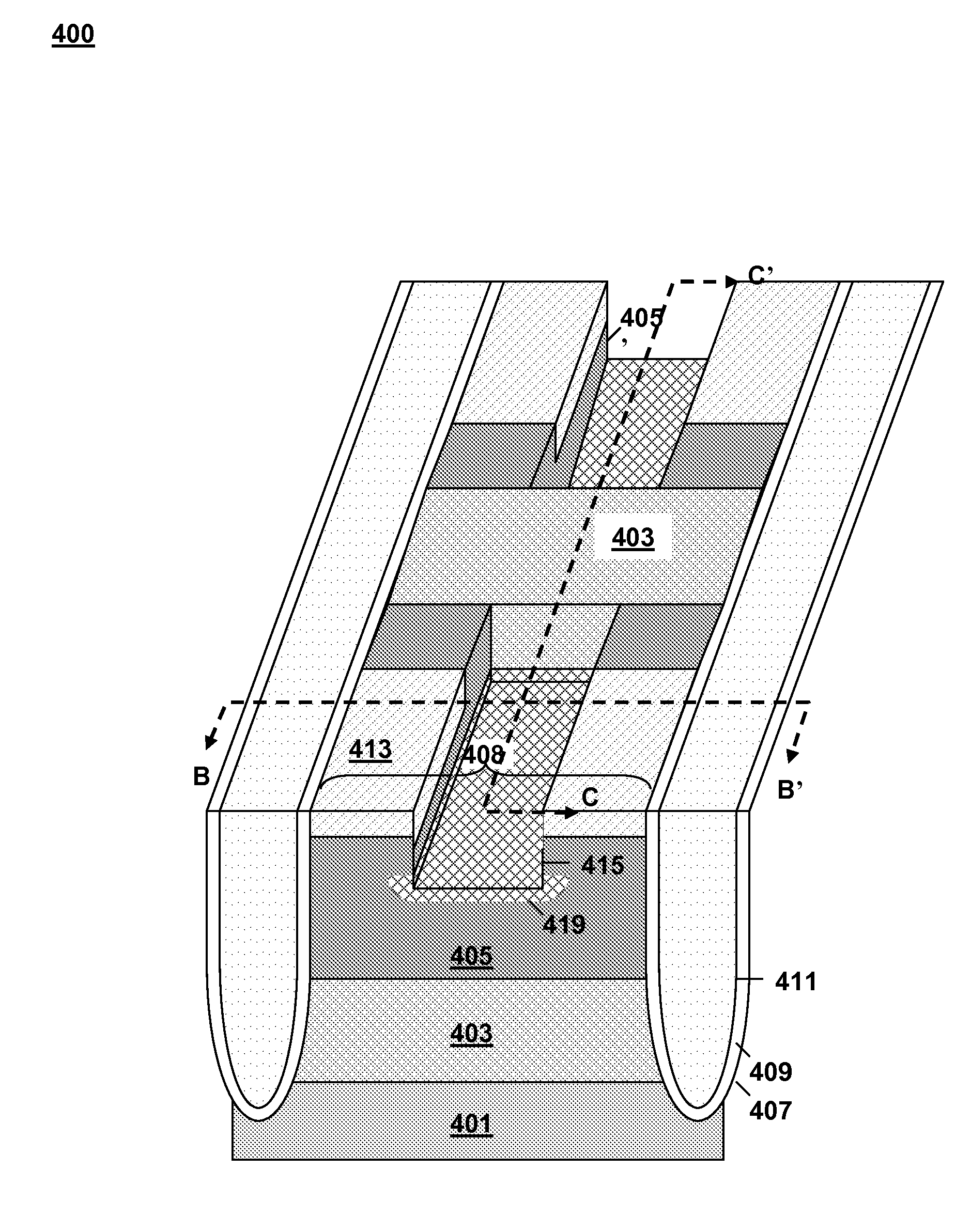
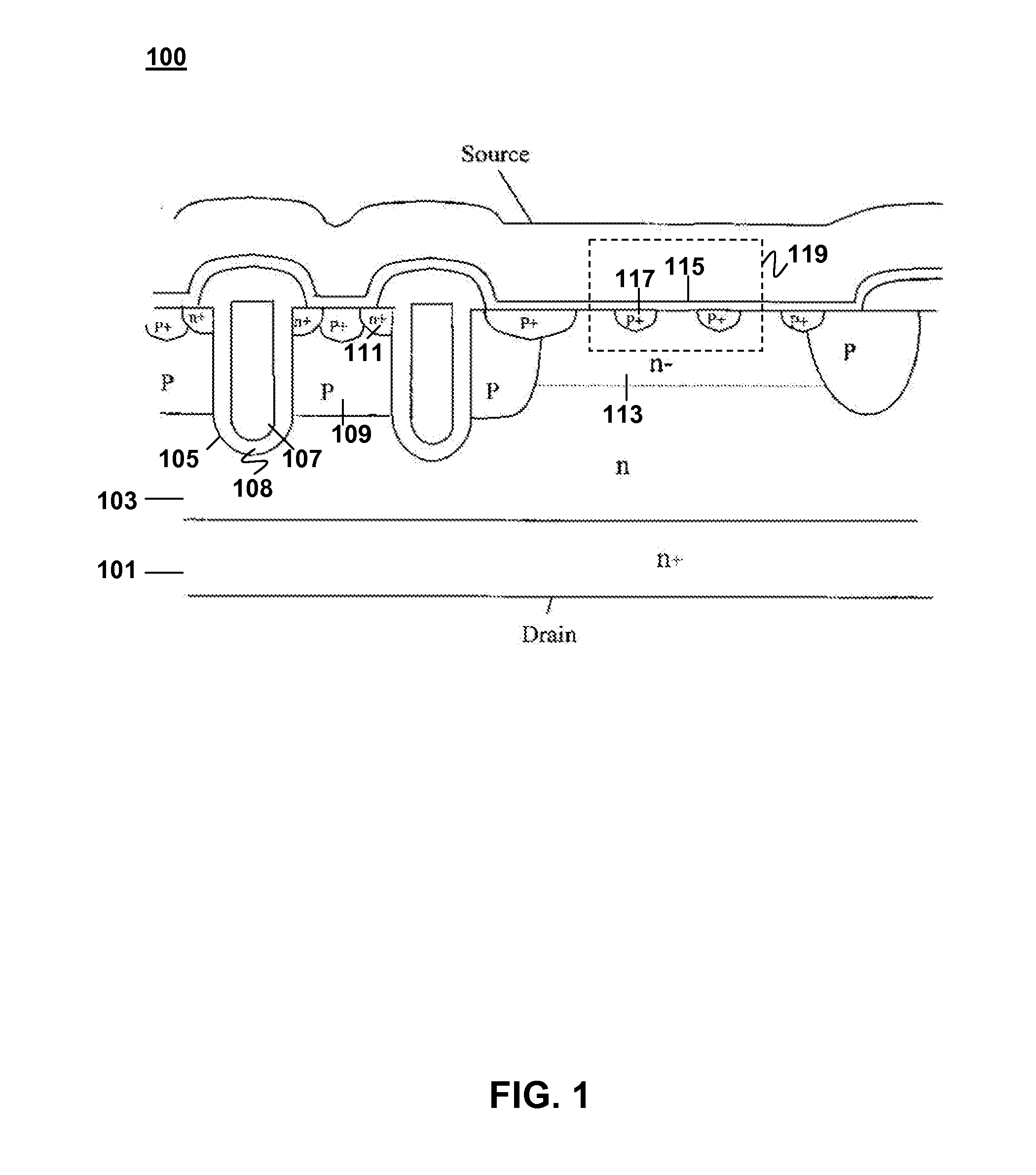
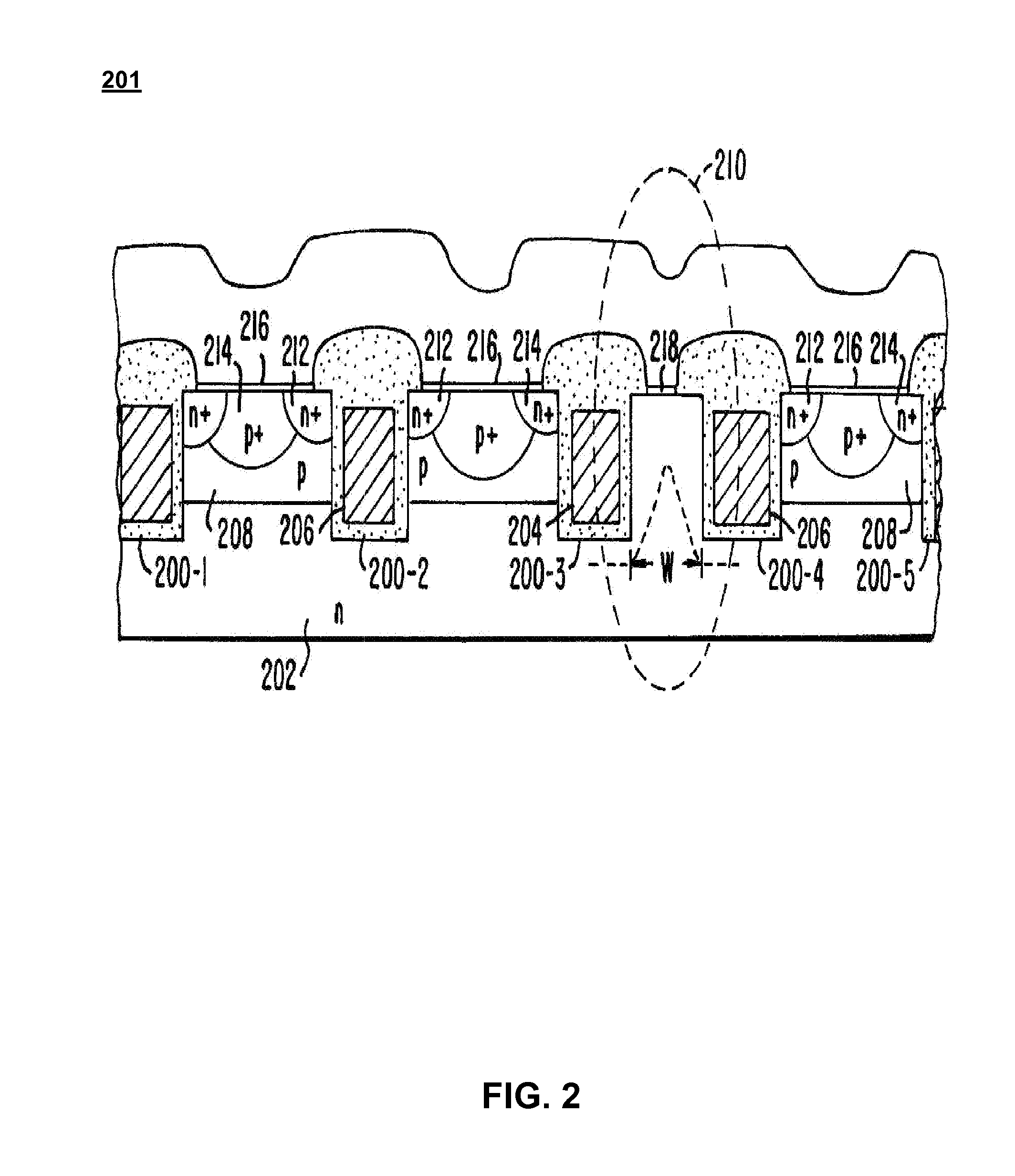
[0020]Several configurations exist for integrating a Schottky diode with a MOSFET to form a power MOSFET. These configurations, however, all suffer from certain undesirable characteristics which make them less than optimal power MOSFET devices. FIGS. 1-3 illustrate three such prior art configurations.

[0021]FIG. 1 illustrates a prior art integrated structure with multiple MOSFET devices and a junction barrier Schottky (JBS) in parallel with those MOSFET devices. The integrated structure 100 includes an n+ type substrate 101 with an n type epitaxial layer 103. Several MOSFETs are built into the integrated structure 100. A trench 105 is fabricated into the epitaxial layer 103 and filled with conductive material 107 surrounded by an insulation layer 108 to form each gate region 107 of each MOSFET in the integrated structure 100. An area of the epitaxial layer 103 surrounding each trench is doped with p-type material to form the body region 109 of each MOSFET. Each body regio...


PUM


Abstract

An integrated structure combines field effect transistors and a Schottky diode. Trenches formed into a substrate composition extend along a depth of the substrate composition forming mesas therebetween. Each trench is filled with conductive material separated from the trench walls by dielectric material forming a gate region. Two first conductivity type body regions inside each mesa form wells partly into the depth of the substrate composition. An exposed portion of the substrate composition separates the body regions. Second conductivity type source regions inside each body region are adjacent to and on opposite sides of each well. Schottky barrier metal inside each well forms Schottky junctions at interfaces with exposed vertical sidewalls of the exposed portion of the substrate composition separating the body regions.

Description

FIELD OF INVENTION[0001]Embodiments of the present invention are related MOSFET devices and more specifically to a new approach for integrating a Schottky diode in a MOSFET device.BACKGROUND OF INVENTION[0002]Schottky diodes have been used to replace P-N junction diodes in many applications. In particular, Schottky diodes have been used to replace P-N junction diodes in power MOSFETs (i.e., MOSFET with body diode in parallel with source and drain). Power MOSFETs that implement P-N junction diodes exhibit several undesirable characteristics, which include: large forward conduction loss, storage of charge between body-epitaxial junction when operating in forward bias, excess stored minority charges which cause large recovery currents and voltage overshoots when the power MOSFET is switched from forward bias to reverse bias, generation of radio frequency interference during fast switching. All of these characteristics cause unnecessary stress to the device, leading to sub-optimal perfo...

Claims


Application Information

Patent Timeline
IPC IPC(8): H01L29/78H01L29/872H01L21/8234
CPCH01L27/0629H01L29/8725H01L29/66734H01L29/7806H01L29/1095H01L29/41766H01L29/7813H01L29/0619H01L29/0623H01L29/872
Inventor LUI, SIKSU, YING, DANIELBHALLA, ANUP
Owner ALPHA & OMEGA SEMICON INC
Why Eureka
Eureka Blog
Learn More