
Display device and driving method thereof

a technology of display device and driving method, which is applied in the direction of electric digital data processing, instruments, computing, etc., can solve the problems of increasing mutual interference between data lines and control lines etc., and achieves simple pixel circuit configuration, reducing manufacturing yield, and reducing brightness deterioration in the el element.

Active Publication Date: 2012-10-04
JDI DESIGN & DEV GK
View PDF3 Cites 1 Cited by
  • Summary
  • Abstract
  • Description
  • Claims
  • Application Information

AI Technical Summary

Benefits of technology

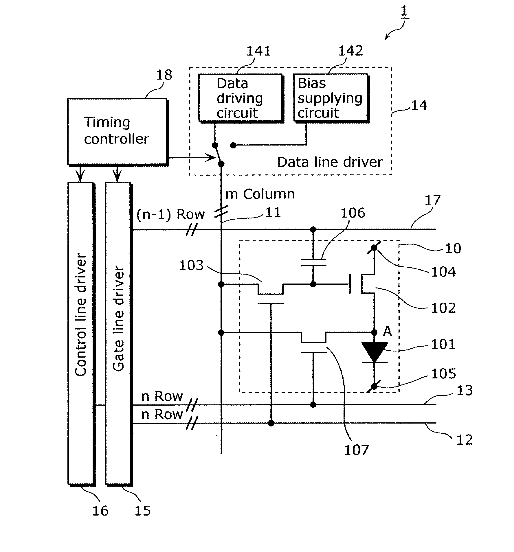
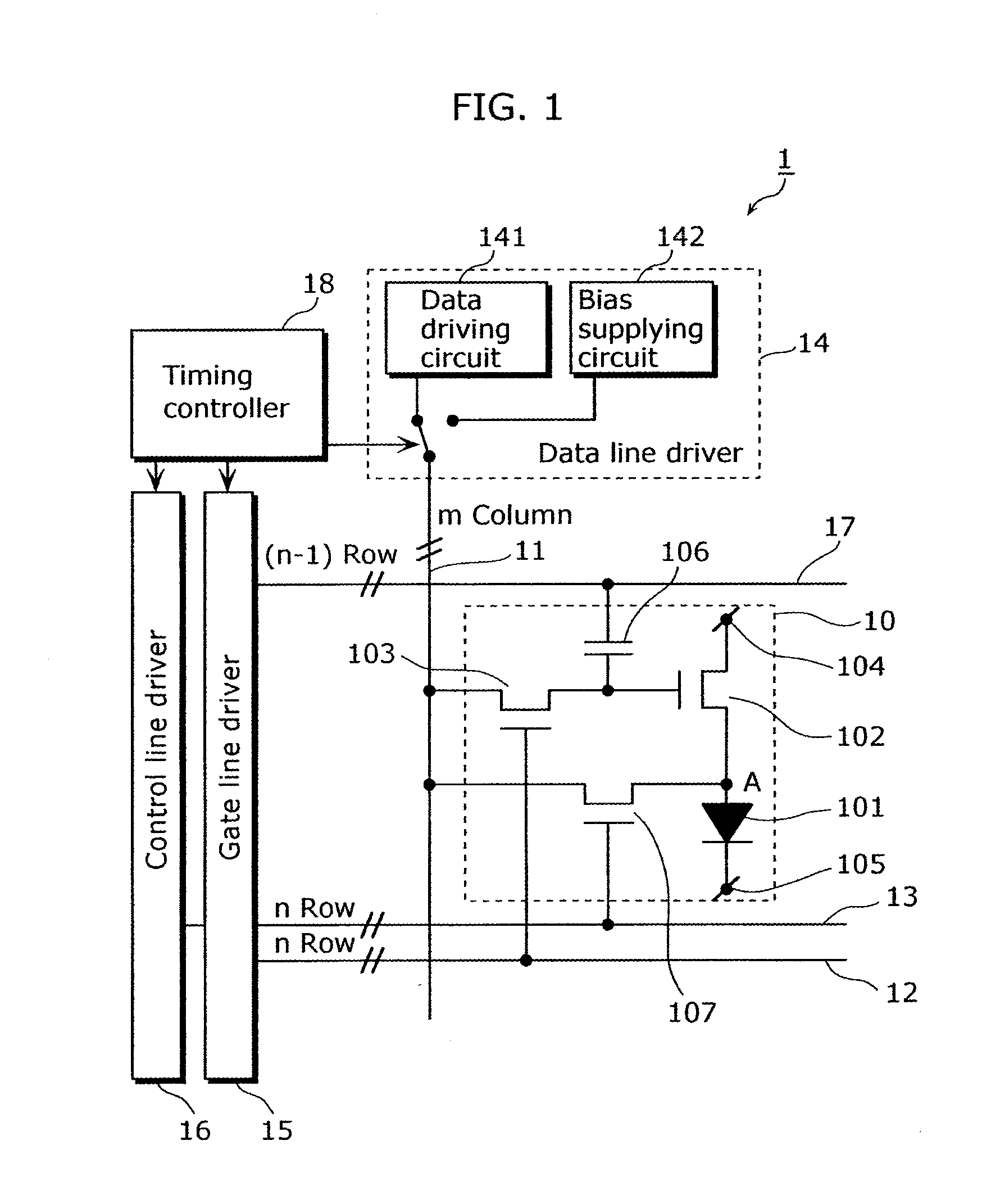
[0014]In view of the aforementioned problem, the present invention has as an object to provide a display device and a driving method thereof, which can implement the reversing of brightness deterioration in the EL element while maintaining display quality, and which has a simple pixel circuit configuration that does not reduce manufacturing yield.
[0033]According to the display device and the driving method thereof in the present invention, part of the basic circuit components for luminescence production is used in-common as an additional circuit required in the application of bias voltage to the luminescence element, and thus the predetermined bias voltage can be provided to the luminescence element without a reduction in manufacturing yield, using a simple pixel circuit configuration. Therefore, the brightness deterioration in the EL element can be reversed while maintaining display quality.

Problems solved by technology

In the case of the above-described circuit configuration, although application of reverse bias voltage to the luminescence element is possible, the increase in the components in the pixel configuration leads to a reduction in manufacturing yield.
In addition, when control lines increase, mutual interference between data lines and control lines increases since the data lines intersect with plural control lines.
As a result of causing an increase in wiring load, such mutual interference becomes the cause for display unevenness attributable to the deterioration of the signal waveform of the data lines.

Method used


Image

  • Display device and driving method thereof
  • Display device and driving method thereof
  • Display device and driving method thereof

Examples


first embodiment

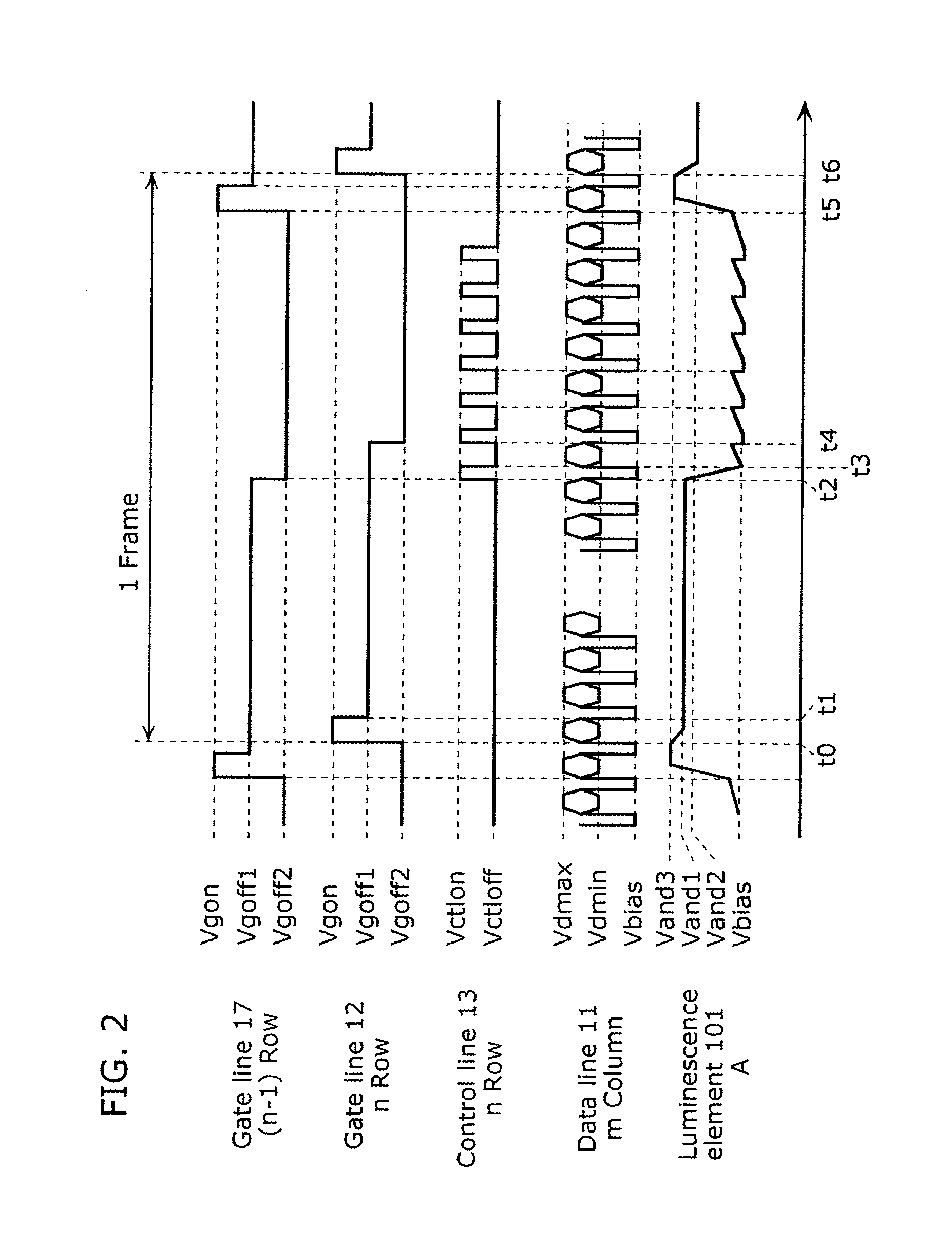
[0047]The display device in the present embodiment includes luminescence elements, data lines, a data driving circuit which supplies signal voltage to the data lines, and a bias supplying circuit which supplies a predetermined bias voltage to the data lines. Each of the luminescence pixels includes a first transistor which converts the signal voltage supplied from a data line into signal voltage, a luminescence element which produces luminescence when signal current flows, a third transistor which switches between conduction and non-conduction between the signal line and the luminescence element, and a capacitance element having one terminal connected to a gate terminal of the first transistor and another terminal connected to a write control line for permitting data writing to a luminescence pixel in a stage that is one row ahead, that is, an immediately preceding luminescence pixel. In a period during which signal current does not flow to the luminescence element, a predetermined ...

second embodiment

[0102]FIG. 5 is a diagram showing the configuration of a luminescence pixel circuit and peripheral circuits thereof in a display device in a second embodiment of the present invention. A display device 2 in the figure includes the luminescence pixel 10, the data line 11, the gate line 12, the control line 13, the data line driver 14, the gate line driver 15, the control line driver 16, a luminescence control line 19, a luminescence control line driver 20, and a timing controller 21. Compared with the display device 1 in the first embodiment, the display device 2 in the figure is different, as a circuit configuration, in terms of having the capacitance element 106, which is a component of the luminescence pixel 10, connected to a dedicated luminescence control line instead of being connected to a gate line which is connected to the luminescence pixel in the preceding stage, and in terms of being provided with a luminescence control line driver which drives such luminescence control l...

third embodiment

[0124]FIG. 7 is a diagram showing the configuration of a luminescence pixel circuit and peripheral circuits thereof in a display device in a third embodiment of the present invention. A display device 3 in the figure includes a luminescence pixel 22, the data line 11, the gate line 12, the control line 13, the data line driver 14, the gate line driver 15, the control line driver 16, and a timing controller 23. Compared with the display device 1 in the first embodiment, the display device 3 in the figure is different, as a circuit configuration, in that the capacitance element 106, which is a component of the luminescence pixel 22, is connected to the other of the source and drain of the driving transistor 102 instead of being connected to a gate line which is connected to the luminescence pixel in the preceding stage. Furthermore, with the difference in this circuit configuration, the drive timing of the timing controller which drives each driver is different. Thus, description of p...


PUM


Abstract

A display device includes luminescence pixels that each include a driving transistor, a luminescence element, and a switching transistor that switches between conduction and non-conduction between a data line and an anode or a cathode of the luminescence element. A data driving circuit supplies a signal voltage to the data line, and a bias supplying circuit supplies a predetermined bias voltage to the data line. A controller applies the predetermined bias voltage to the anode or the cathode of the luminescence element by causing a non-conduction state between the data line and the data driving circuit, causing a conduction state between the data line and the bias supplying circuit, and switching the switching transistor ON within a period in which a signal current does not flow to the luminescence element.

Description

CROSS REFERENCE TO RELATED APPLICATION[0001]The present application is a continuation application of U.S. patent application Ser. No. 12 / 713,491 filed on Feb. 26, 2010, which is a continuation application of PCT Application No. PCT / JP2009 / 002303 filed May 26, 2009, designating the United States of America, the disclosure of each of which, including the specification, drawings, and claims, is incorporated herein by reference in its entirety.[0002]The disclosure of Japanese Patent Application No. 2008-141715 filed on May 29, 2008, including specification, drawings, and claims, is also incorporated herein by reference in its entirety.BACKGROUND OF THE INVENTION[0003]1. Field of the Invention[0004]The present invention relates to display devices and driving methods thereof, and particularly to a display device using current-driven luminescence elements, and a driving method thereof.[0005]2. Description of the Related Art[0006]Conventionally, advancements in brightness, vividness, flatne...

Claims


Application Information

Patent Timeline
Patent Type & Authority Applications(United States)
IPC IPC(8): G09G5/00
CPCG09G3/3233G09G2300/0842G09G2310/0262G09G2310/0256G09G2310/0251
Inventor NAKAMURA, MIKAMASUMOTO, KENICHI
Owner JDI DESIGN & DEV GK
Learn More