Optical waveguide device and module

a waveguide and optical waveguide technology, applied in the field of optical waveguide devices and modules, can solve the problems of increasing the degree of integration, device size and power consumption, etc., and achieve the effects of suppressing crosstalk, suppressing crosstalk, and restrainting crosstalk

Active Publication Date: 2012-10-04
NTT ELECTORNICS CORP +1
View PDF5 Cites 30 Cited by
  • Summary
  • Abstract
  • Description
  • Claims
  • Application Information

AI Technical Summary

Benefits of technology

[0023]According to the present invention, in a waveguide device, a cladding and a core are removed at any position on a substrate to form a groove on an optical waveguide. The groove is filled with a material (light blocking material) that attenuates the intensity of light, to terminate the optical waveguide. Thus, light input to the termination structure is attenuated by the light blocking material, suppressing crosstalk which possibly effects on other optical devices. Thus, the present invention can restrain crosstalk occurred in optical devices integrated in the same substrate and can also suppress crosstalk which possibly effects on any other optical device connected directly to the substrate, for example, any other waveguide device or light receiving or emitting element. This is very effective in implementing an optical device with a high degree of integration and is expected to contribute significantly to developing a large-capacity optical communication network that requires control of various optical signals.

Problems solved by technology

For further reduced device size and power consumption and further increased scale, a major challenge is to further increase the degree of integration.

Method used


Image

  • Optical waveguide device and module
  • Optical waveguide device and module
  • Optical waveguide device and module

Examples


example 1

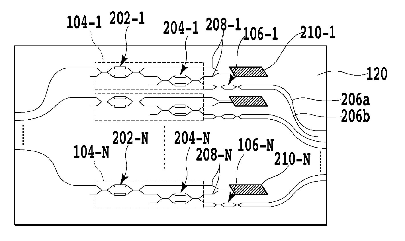
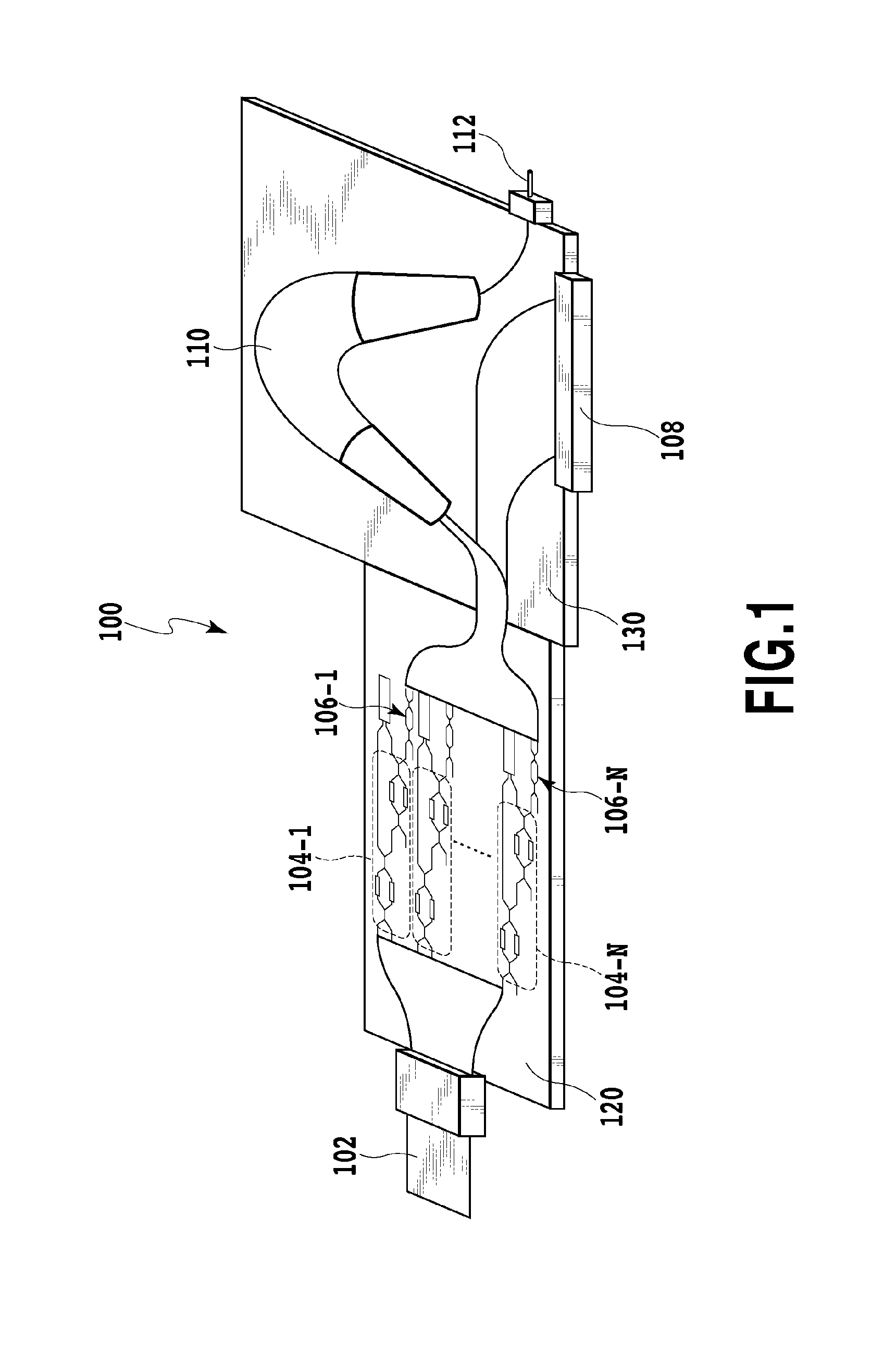
[0059]FIG. 1 is a diagram showing a configuration of a waveguide device according to an example of the present invention. As shown in FIG. 1, a device 100 includes a substrate 120 with VOAs 104-1 to 104-N and a substrate 130 connected to the substrate 120 and is with an arrayed waveguide grating (AWG) 110. The device 100 is configured as a wavelength multiplexing device with an optical level adjustment function (VMUX: VOA equipped MUX). The device is introduced into, for example, a WDM system. In the present configuration example, the VOAs 104-1 to 104-N and tapping optical couplers 106-1 to 106-N are integrated together in one substrate. An optical power monitor PD 108 and the AWG 110 are integrated together in another substrate 130.

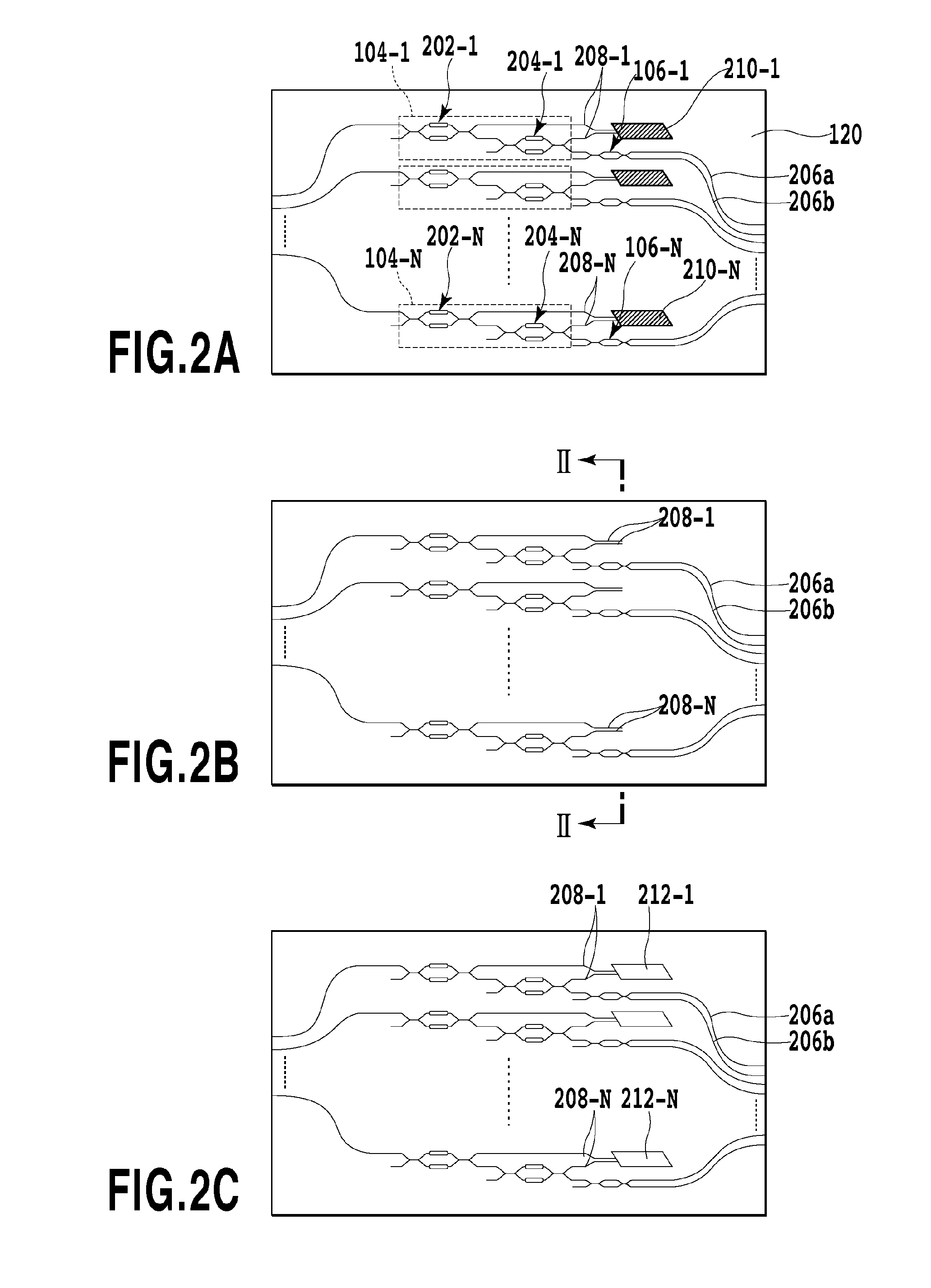
[0060]FIG. 2A is a detailed circuit layout of the substrate 120 with the VOAs 104-1 to 104-N according to the present example. In FIG. 1 and FIGS. 2A to 2C, for simplification of drawing, only thin film heaters that drive the VOAs 104-1 to 104-N are sho...

example 2

[0071]Example 2 of the present invention used a configuration similar to that shown in FIG. 1 and FIG. 2A and in which the light blocking material provided at the terminal of each of the dummy ports 208-1 to 208-N for the VOAs 104-1 to 104-N was a mixture of a silicone resin as a base material and powder metal microparticles that are also used as a pigment. The optical power of light which inputs the light blocking material is attenuated by optical scattering caused mainly by the metal microparticles. The sample prepared was formed of a silica optical waveguide fabricated on a silicon substrate as is the case with Example 1 and included the termination structures 210-1 to 210-N each with a groove and the light blocking material which was introduced in order to prevent light from coupling to the adjacent waveguide and causing crosstalk. Also in the present example, the adjacent channel crosstalk had a value of at most −60 dB.

[0072]Furthermore, the angle of the incidence plane on the ...

example 3

[0073]Example 3 of the present invention used a configuration similar to that in Example 2 and in which the angle of the incidence plane on the groove for the terminated waveguide (the angle θ in FIG. 3) was set equal to Brewster's angle. The other components and the light blocking material were similar to those in Example 2. The Brewster's angle in the present example was calculated to be about 50 degrees. By setting the angle of the incidence plane equal to the Brewster's angle, all the polarization components that are horizontal to the substrate are allowed to input into the light blocking material, and some of the polarization components that are vertical to the substrate are radiated into the waveguide substrate by reflection. Furthermore, equivalent effects are obtained with a near angle to the Brewster's angle or with an angle equal to or larger than the Brewster's angle. Thus, the adverse effect of crosstalk caused by radiated light is further reduced throughout the waveguid...


PUM


Abstract

In a waveguide device, unnecessary optical power is appropriately terminated. According to an embodiment of the present invention, the waveguide device has a termination structure filled with a light blocking material to terminate light from a waveguide end. In the termination structure, a cladding and a core are removed to form a groove on an optical waveguide. The groove is filled with a material (light blocking material) that attenuates the intensity of light. Thus, light input to the termination structure is attenuated by the light blocking material, suppressing crosstalk which possibly effects on other optical devices. Thus, such a termination structure can restrain crosstalk occurred in optical devices integrated in the same substrate and can also suppress crosstalk which possibly effects on any other optical device connected directly to the substrate.

Description

TECHNICAL FIELD[0001]The present invention relates to an optical device using a waveguide on a substrate. More specifically, the present invention relates to a technique to terminate a waveguide that is not connected to an input or output fiber, in any place in the substrate to attenuate the intensity of an optical signal propagating through the waveguide.BACKGROUND ART[0002]With the explosive spread of broadband communication at homes, network contents are being increasingly diversified. This results in increased communication traffic and improved communication service, leading to daily growing needs for increased capacities and speeds and enhanced functions of communication networks, which support the increased traffic and the improved communication service. In recent years, optical communication techniques have played an important role for meeting these needs. Conventional optical networks are mostly terrestrial communication systems that connect two points together based on opti...

Claims


Application Information

Patent Timeline
Patent Type & Authority Applications(United States)
IPC IPC(8): G02B6/12G02B6/35G02B6/28G02B6/00
CPCG02B6/12019G02B6/30G02B6/2552G02B6/12G02B6/305G02B2006/12195G02B6/1228G02B6/124G02B6/243G02B2006/12126G02B2006/12142G02B2006/12145G02B2006/1215G02B6/12016
Inventor ISHIKAWA, TAKANORISHIBAZAKI, TOMOYONAGANO, MITSURUYANAGISAWA, MASAHIROTERUI, HIROSHIITOH, MIKITAKA
Owner NTT ELECTORNICS CORP
Why Eureka
Try Eureka