Semiconductor inspecting apparatus

a technology of electromagnetic radiation and electromagnetic radiation, applied in semiconductor/solid-state device testing/measurement, instruments, nuclear engineering, etc., can solve problems such as throughput degradation, and achieve the effect of preventing position deviation and preventing position deviation

Active Publication Date: 2012-10-18
HITACHI HIGH-TECH CORP
View PDF1 Cites 4 Cited by
  • Summary
  • Abstract
  • Description
  • Claims
  • Application Information

AI Technical Summary

Benefits of technology

[0022]As set for the above, the present invention can provide a semiconductor inspecting apparatus capable of preventing a position deviation occurring when inspecting an outer peripheral portion of a sample. Further, the present invention can provide application apparatuses such as an electronic drawing apparatus, etc., capable of preventing the position deviation occurring when patterns are drawn at the outer peripheral portion of the sample.

Problems solved by technology

However, when the position deviation is large, the movement amount to the positions to be measured is increased since the position adjusted by using the mechanical stage and the position adjusted by using the SEM phase are far away from each other, thereby causing the degradation in throughput.

Method used


Image

  • Semiconductor inspecting apparatus
  • Semiconductor inspecting apparatus
  • Semiconductor inspecting apparatus

Examples


first embodiment

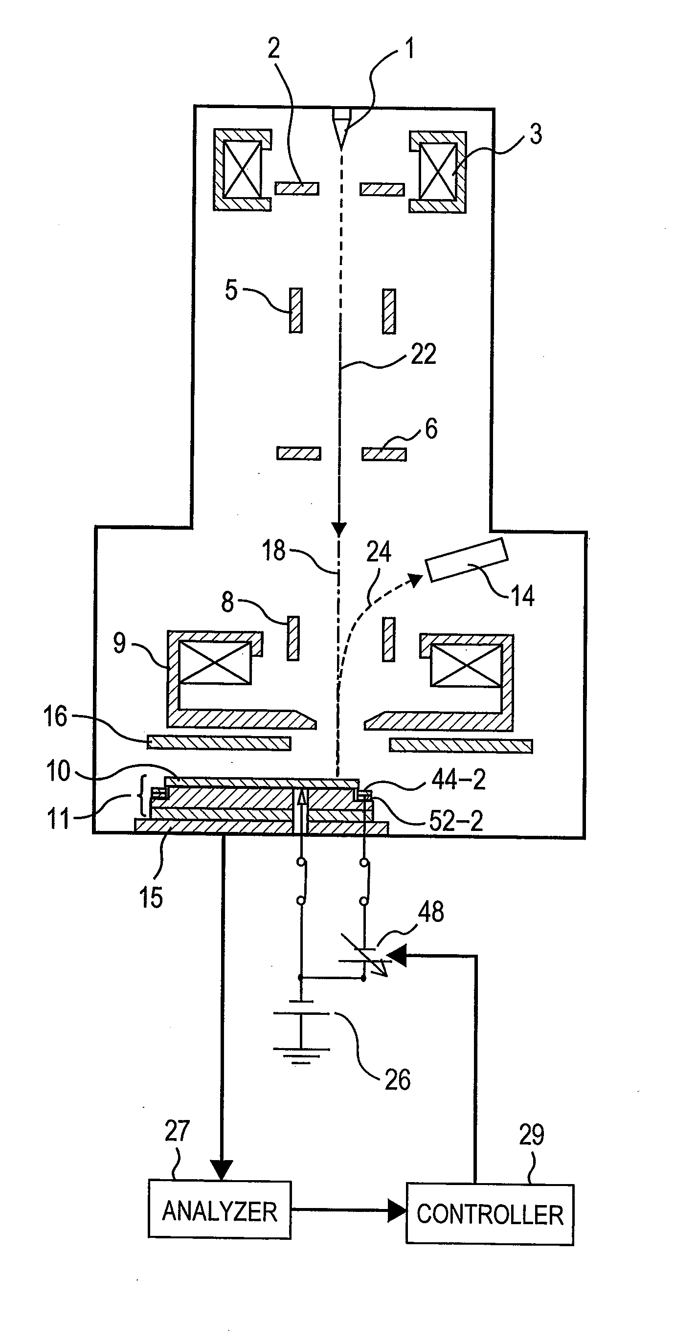
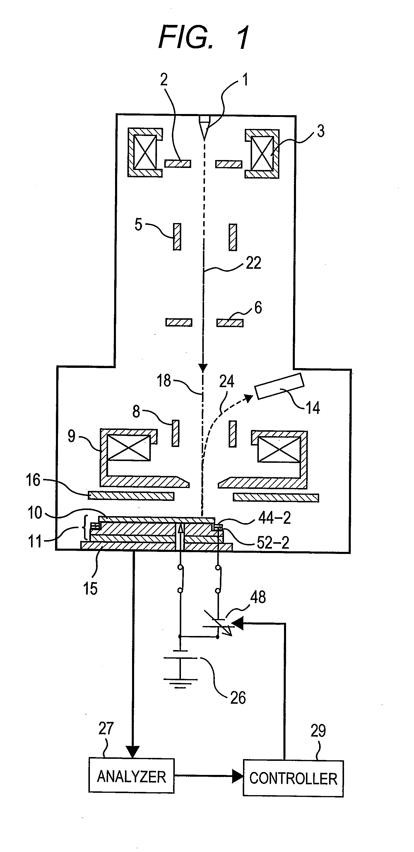
[0044]Hereinafter, a first embodiment is an example of a semiconductor inspection apparatus using a charged particle beam applied to the present invention and a first embodiment applied to a CD-SEM will be described in detail with reference to FIGS. 1 to 5.

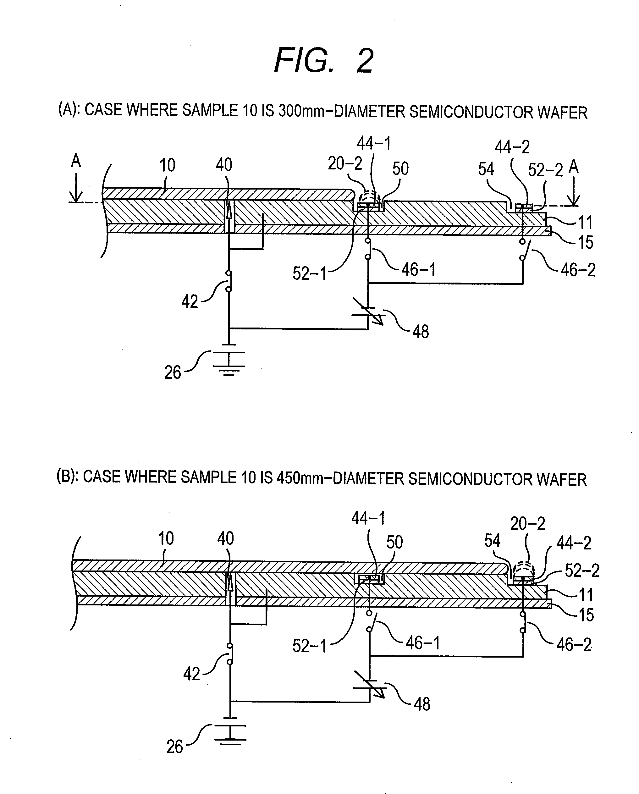
[0045]FIG. 1 is a schematic diagram of an electron optical system of a CD-SEM. In addition, FIG. 2 is an enlarged diagram of a vicinity of a sample stage 11 used in a CD-SEM of the present embodiment. Among others, FIG. 2(A) shows a structure when a wafer of φ300 as a sample 10 is installed on the sample stage 11. In addition, FIG. 3 is a diagram showing a cross section of line A-A of the sample stage 11 used in the present embodiment of FIG. 2. Further, in order to easily facilitate the position relationship, an inner edge of a groove 50, an outer edge of the groove 50, and an inner edge of a concave portion 54 are shown by a dotted line. Further, FIG. 4 shows a structure of a vicinity of a sample stage 11, a shield electrode 16,...

second embodiment

[0062]Next, a second embodiment of the present invention will be described with respect to only portions different from the first embodiment. Although the first exemplary of the present invention installs the sample 10 on the sample stage 11, it does not attract the sample 10. On the other hand, the second embodiment uses the electrostatic chuck as the sample stage 11 to attract the sample 10 into the sample stage 11 and firmly hold the sample thereto. Hereinafter, the structure of the second embodiment will be described with reference to FIGS. 6 to 8.

[0063]FIGS. 6A and 6B each are a diagram showing a structure of the vicinity of the sample stage 11 when the sample 10 having a first size, i.e., the wafer of φ300 as the sample is installed on the sample stage 11 and when the sample 10 having a second size, i.e., the wafer ofφ450 as the sample is installed on the sample stage 11, respectively. In addition, FIG. 7 is a top view showing a cross-sectional view taken along line B-B of the...

third embodiment

[0077]Next, a third embodiment of the present invention will be described with respect to only portions different from the second embodiment. The second embodiment forms the groove 50 or the concave part 54 on the surface of the dielectric portion 34 of the sample stage 11 that is the electrostatic chuck and the bottom surface thereof is provided with the potential correcting electrode 44-1 and the potential correcting electrode 44-2, respectively. In this case, in addition to the process of manufacturing the sample stage 11 having the general electrostatic chuck structure, the process of forming the groove 50 and the concave part 54 in the dielectric portion 34 and the process of forming the potential correcting electrode 44-1 and the potential correcting electrode 44-2 are newly needed. Therefore, the third embodiment has a relatively simple structure. The third embodiment installs the potential correcting electrode 44-1 and the potential correcting electrode 44-2 at the position ...


PUM


Abstract

In the case of inspecting samples having different sizes by means of a semiconductor inspecting apparatus, a primary electron beam bends since distribution is disturbed on an equipotential surface at the vicinity of the sample at the time of inspecting vicinities of the sample, and what is called a positional shift is generated. A potential correcting electrode is arranged outside the sample and at a position lower than the sample lower surface, and a potential lower than that of the sample is applied. Furthermore, a voltage to be applied to the potential correcting electrode is controlled corresponding to a distance between the inspecting position and a sample outer end, sample thickness and irradiation conditions of the primary electron beam.

Description

[0001]This application is a continuation of U.S. patent application Ser. No. 13 / 000,461, filed Dec. 21, 2010, which is a 371 of international Application No. PCT / JP2009 / 002860, filed Jun. 23, 2009, and which claims priority to Japanese Application No. 2008-165757, filed Jun. 25, 2008.TECHNICAL FIELD[0002]The present invention relates to a semiconductor inspecting apparatus using a charged particle beam used for manufacturing a semiconductor device.BACKGROUND ART[0003]In order to measure a dimension of contact holes between wiring layers or gate electrodes in manufacturing a semiconductor device, an inspecting apparatus using a primary electron beam such as a critical-dimension scanning electron microscope (hereinafter, referred to as a CD-SEM) has been used as one type of charged particle beam application apparatuses.[0004]Herein, FIG. 14 schematically shows an electron optical system of an SEM semiconductor inspecting apparatus used in the related art.[0005]A primary electron beam ...

Claims


Application Information

Patent Timeline
Patent Type & Authority Applications(United States)
IPC IPC(8): H01J37/20
CPCH01J37/265H01J37/28H01J37/20H01L22/12H01J2237/0044H01L22/10H01J2237/2817H01L2924/0002H01L2924/00H01L22/00
Inventor MIYA, GOKANNO, SEIICHIROKITSUNAI, HIROYUKIMATSUSHIMA, MASARUSHUTO, TORU
Owner HITACHI HIGH-TECH CORP
Why Eureka
Try Eureka