
Parallel Image Processing System

a parallel image processing and parallel image technology, applied in the field of parallel image processing system, can solve the problems of insufficient manufacturing cost effectiveness, large size of the mask, and insufficient processing of the entire rectangle substra

Active Publication Date: 2012-10-18
APPLIED MATERIALS INC
View PDF2 Cites 5 Cited by
  • Summary
  • Abstract
  • Description
  • Claims
  • Application Information

AI Technical Summary

Benefits of technology

[0009]System and method for a parallel image processing mechanism for applying mask data patterns to substrate in a lithography manufacturing process are disclosed. In one embodiment, the parallel image processing system includes a graphics engine configured to process one or more graphical objects to generate a plurality of convex polygons, and to form an edge list for representing each of the plurality of convex polygons, a distributor configured to distribute the edge list to a plurality of

Problems solved by technology

However, they are entirely different from the manufacturing perspective.
For the IC industry, a primary challenge is small CD features can be produced on a round 300 mm wafer.
But for the FPD industry, one primary challenge is how large an entire rectangle substrate can be processed.
In one viewpoint, one of the main challenges for FPD manufacturing is to keep throughput in pace with justifiable economics for each successive generation.
The size of the mask is too large to be manufactured cost effectively.
By contrast, parallel scanning for mask-less lithography demands different challenges.

Method used


Image

  • Parallel Image Processing System
  • Parallel Image Processing System
  • Parallel Image Processing System

Examples


Embodiment Construction

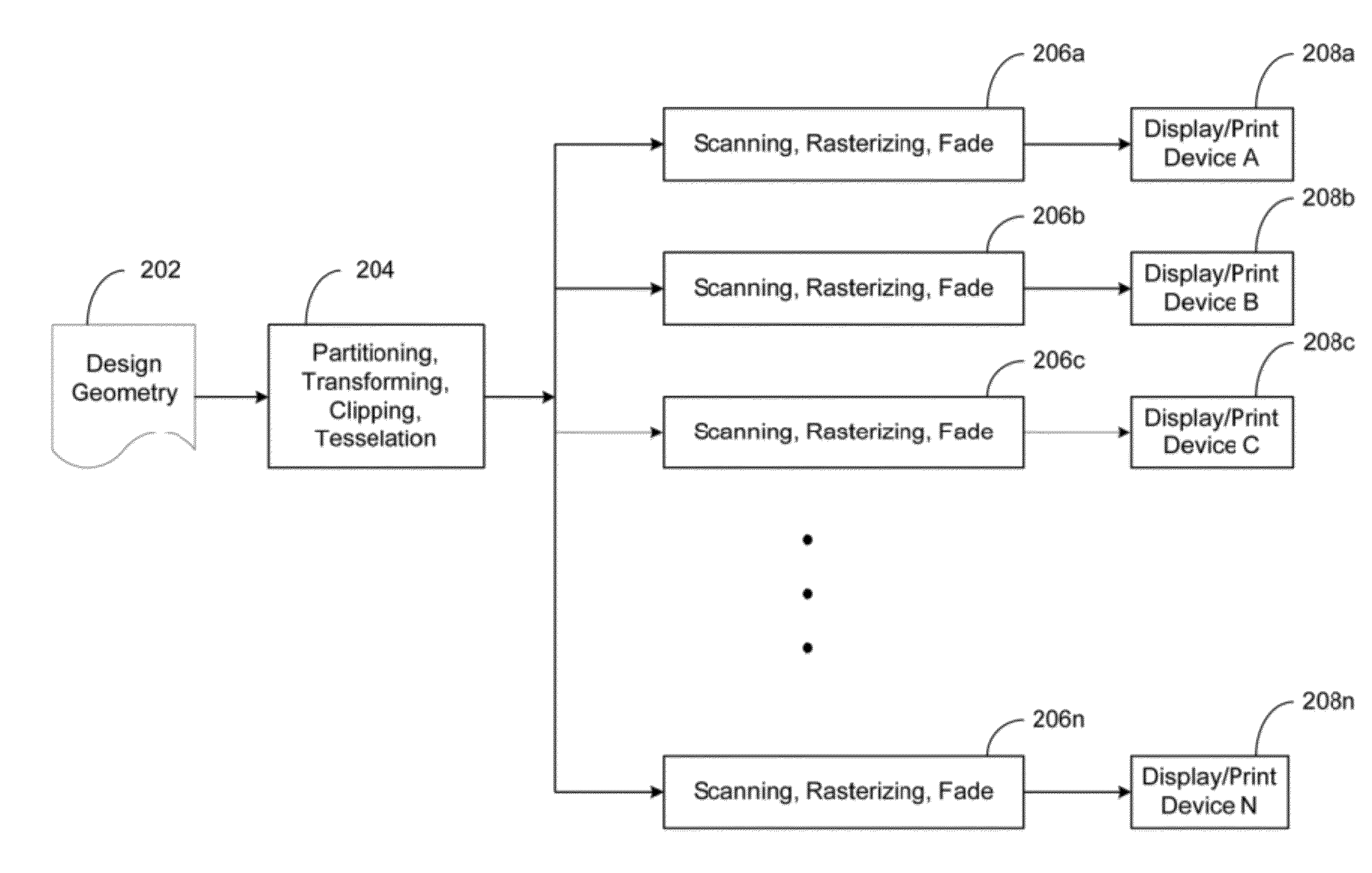
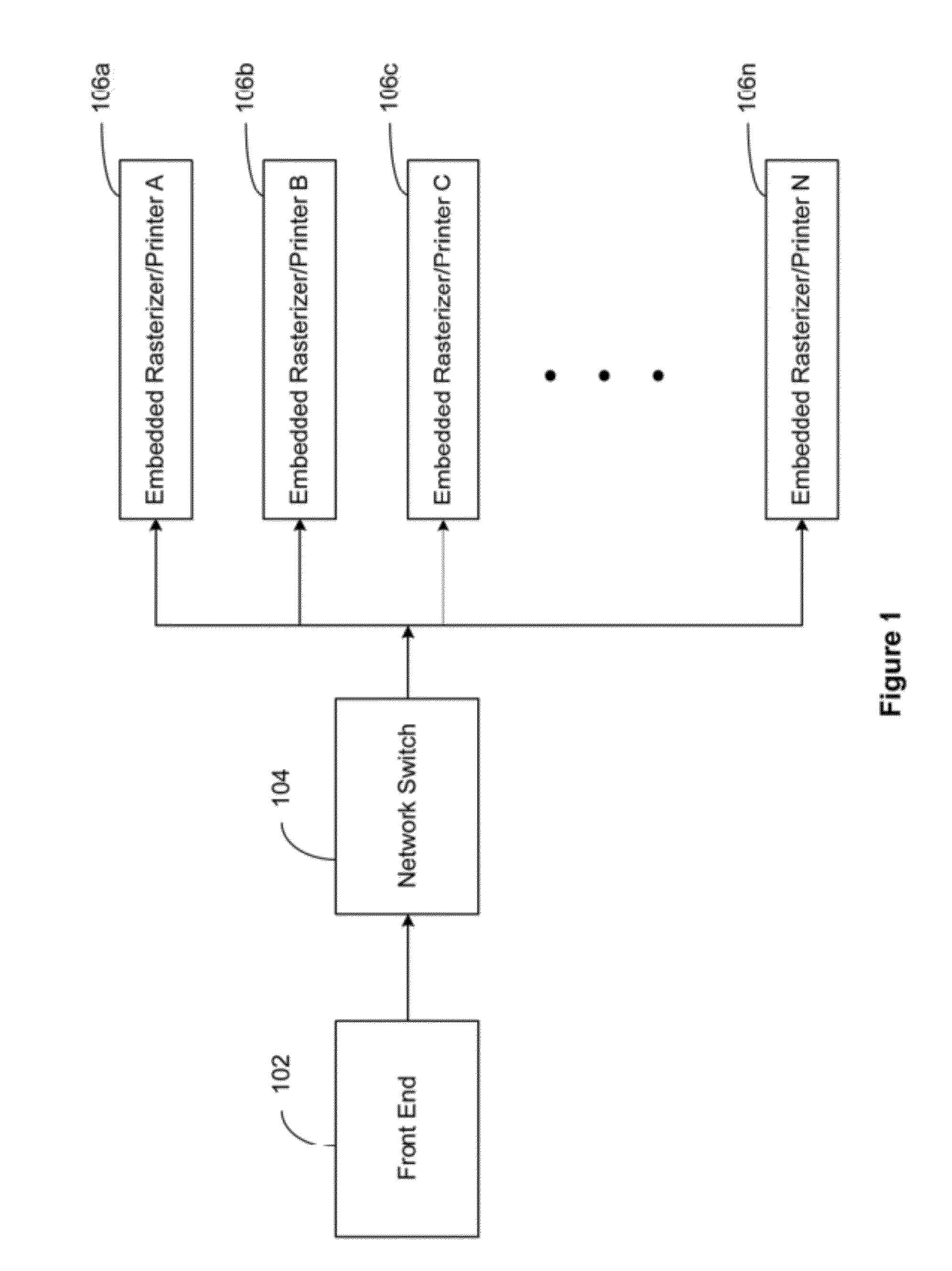
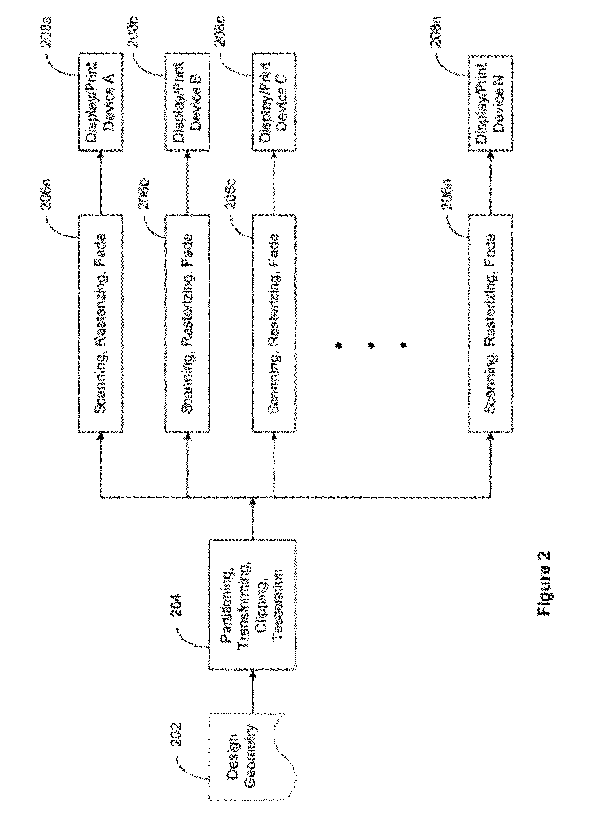
[0031]System and method are provided for a parallel image processing mechanism for applying mask data patterns to substrate in a lithography manufacturing process. The following descriptions are presented to enable any person skilled in the art to make and use the invention. Descriptions of specific embodiments and applications are provided only as examples. Various modifications and combinations of the examples described herein will be readily apparent to those skilled in the art, and the general principles defined herein may be applied to other examples and applications without departing from the spirit and scope of the invention. Thus, the present invention is not intended to be limited to the examples described and shown, but is to be accorded the widest scope consistent with the principles and features disclosed herein.

[0032]Some portions of the detailed description that follows are presented in terms of flowcharts, logic blocks, and other symbolic representations of operations...


PUM


Abstract

System and method for a parallel image processing mechanism for applying mask data patterns to substrate in a lithography manufacturing process are disclosed. In one embodiment, the parallel image processing system includes a graphics engine configured to partition an object into a plurality of trapezoids and form an edge list for representing each of the plurality of trapezoids, and a distributor configured to receive the edge list from the graphics engine and distribute the edge list to a plurality of scan line image processing units. The system further includes a sentinel configured to synchronize operations of the plurality of scan line image processing units, and a plurality of buffers configured to store image data from corresponding scan line image processing units and outputs the stored image data using the sentinel.

Description

CROSS REFERENCE TO RELATED APPLICATIONS[0001]This application claims the benefit of U.S. provisional application No. 61 / 346,436, “A Parallel Imaging Processing System” filed May 19, 2010. The aforementioned United States application is hereby incorporated by reference in its entirety.FIELD OF THE INVENTION[0002]The present invention relates to the field of computer imaging processing. In particular, the present invention relates to system that employs a parallel image processing mechanism for applying mask data patterns to substrate in a lithography manufacturing process.BACKGROUND OF THE INVENTION[0003]Fast-paced technology progress in semiconductor integrated circuit (IC) industry has benefited well for the manufacturing of active matrix liquid crystal display (AMLCD) TV and computer monitor displays. In the recent years, the size of LCD TV and computer monitor displays has grown to be larger and yet more affordable.[0004]In the semiconductor IC industry, a technology generation i...

Claims


Application Information

Patent Timeline
IPC IPC(8): G06F15/80
CPCG06T11/40G03F7/70425G06T1/20
Inventor KEANE, BARRYLAIDIG, THOMAS
Owner APPLIED MATERIALS INC
Learn More