Spin transport device

a technology of transport device and spin, which is applied in the direction of semiconductor device, basic electric element, electrical apparatus, etc., can solve the problem of small output and achieve the effect of improving output, high detection efficiency and high spin injection efficiency

Active Publication Date: 2012-10-25
TDK CORPARATION
View PDF5 Cites 11 Cited by
  • Summary
  • Abstract
  • Description
  • Claims
  • Application Information

AI Technical Summary

Benefits of technology

[0015]The impurity concentration in the second region is higher than that in the first region, but when the impurity concentrations are in the ranges described above, there is an effect that flow of the spin current toward the second region increases.
[0016]Each of the first and second tunnel barrier layers is formed of MgO, Al2O3, SiO2, ZnO, or MgAl2O4. These materials have an advantage in that efficiency of spin injection and detection is high.
[0017]According to the spin transport device in an aspect of the present invention, it is possible to improve the output since the spin current can be unevenly distributed in the region in an output direction due to a difference in impurity concentration.

Problems solved by technology

However, in the non-local structure type semiconductor spin transport device, there is a problem in that an output is generally small.

Method used


Image

  • Spin transport device
  • Spin transport device
  • Spin transport device

Examples


Embodiment Construction

[0044]Hereinafter, a spin transport device according to embodiments will be described. The same reference numerals are given to the same elements, and duplicate explanation thereof will be omitted.

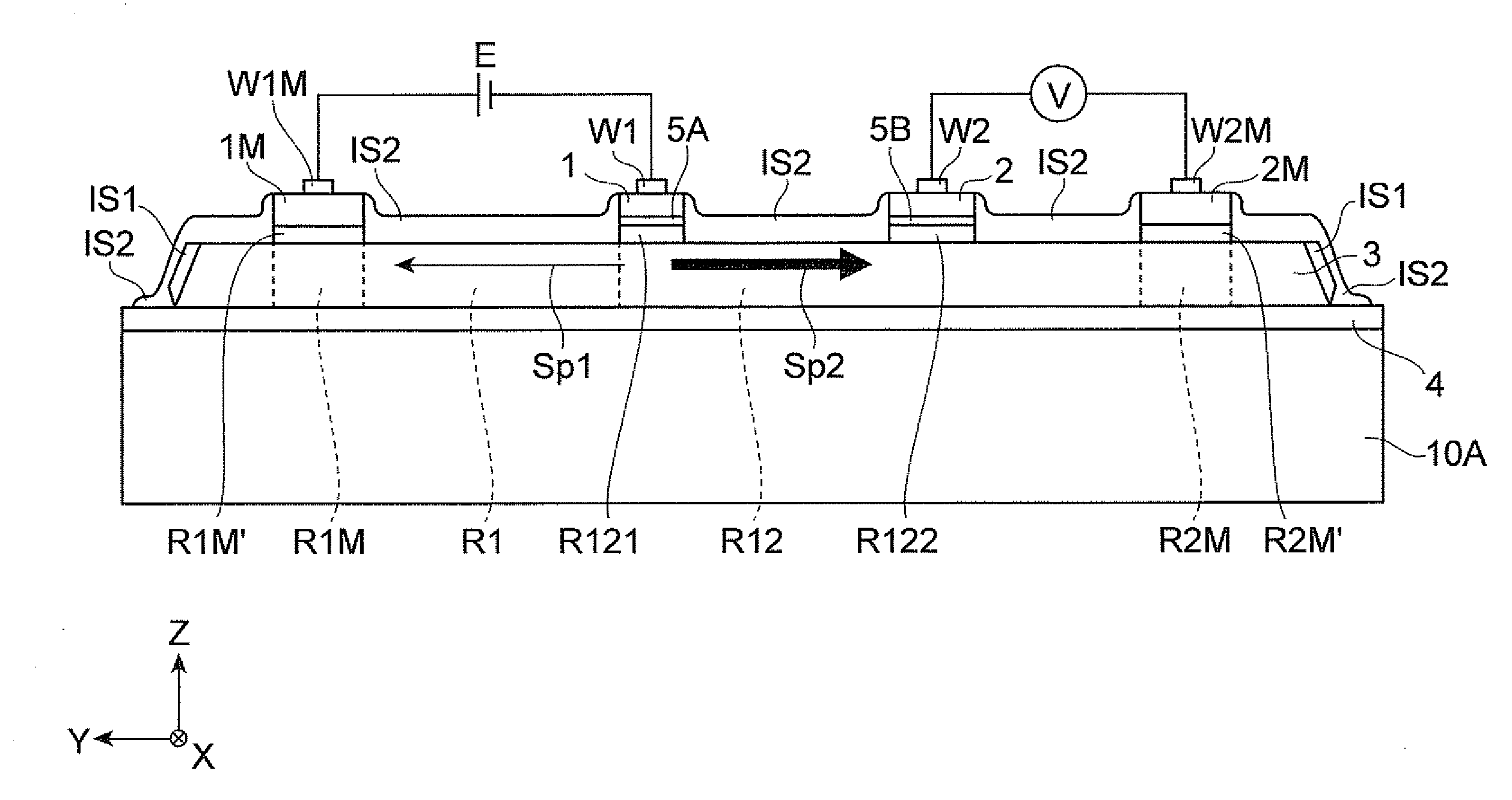
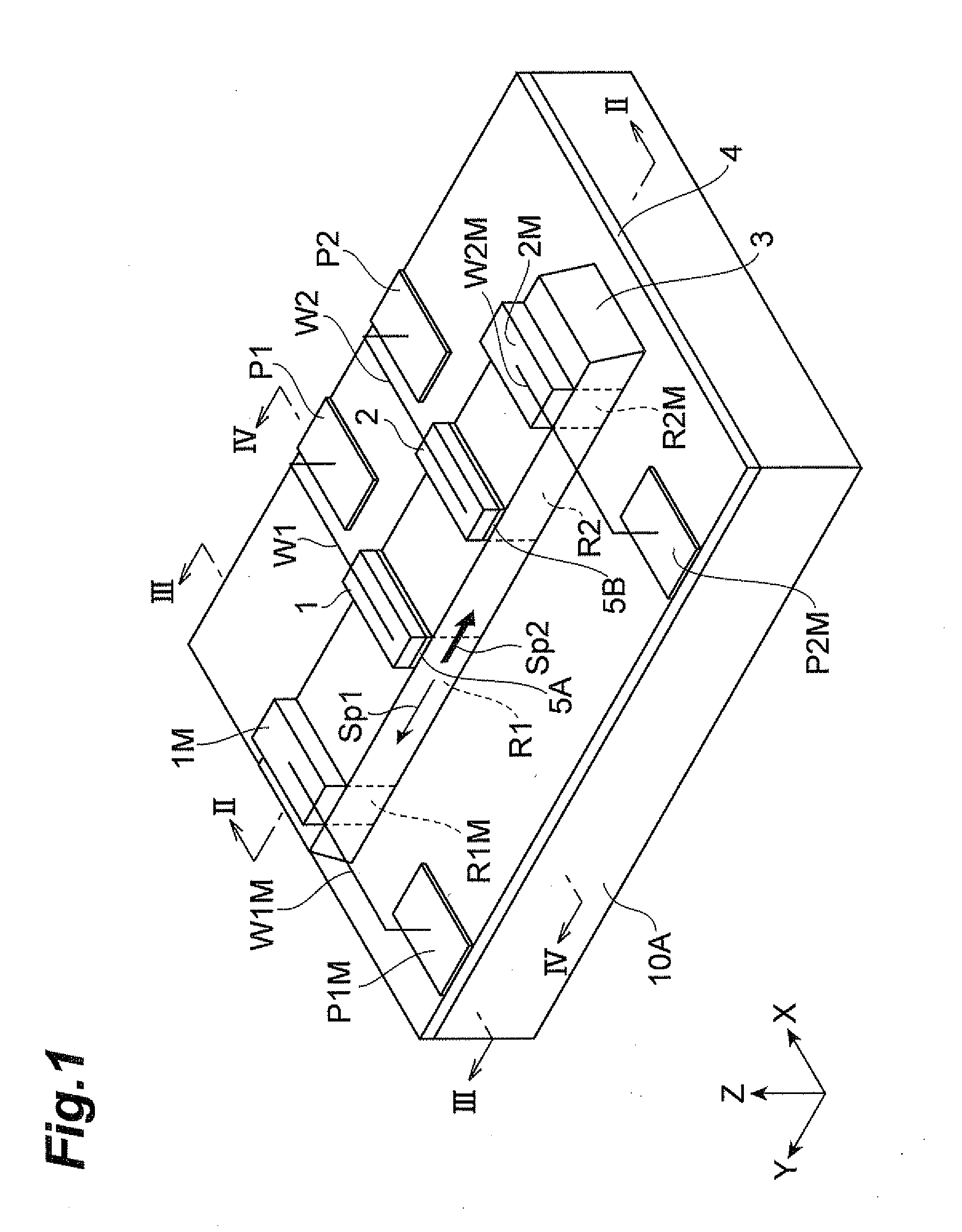
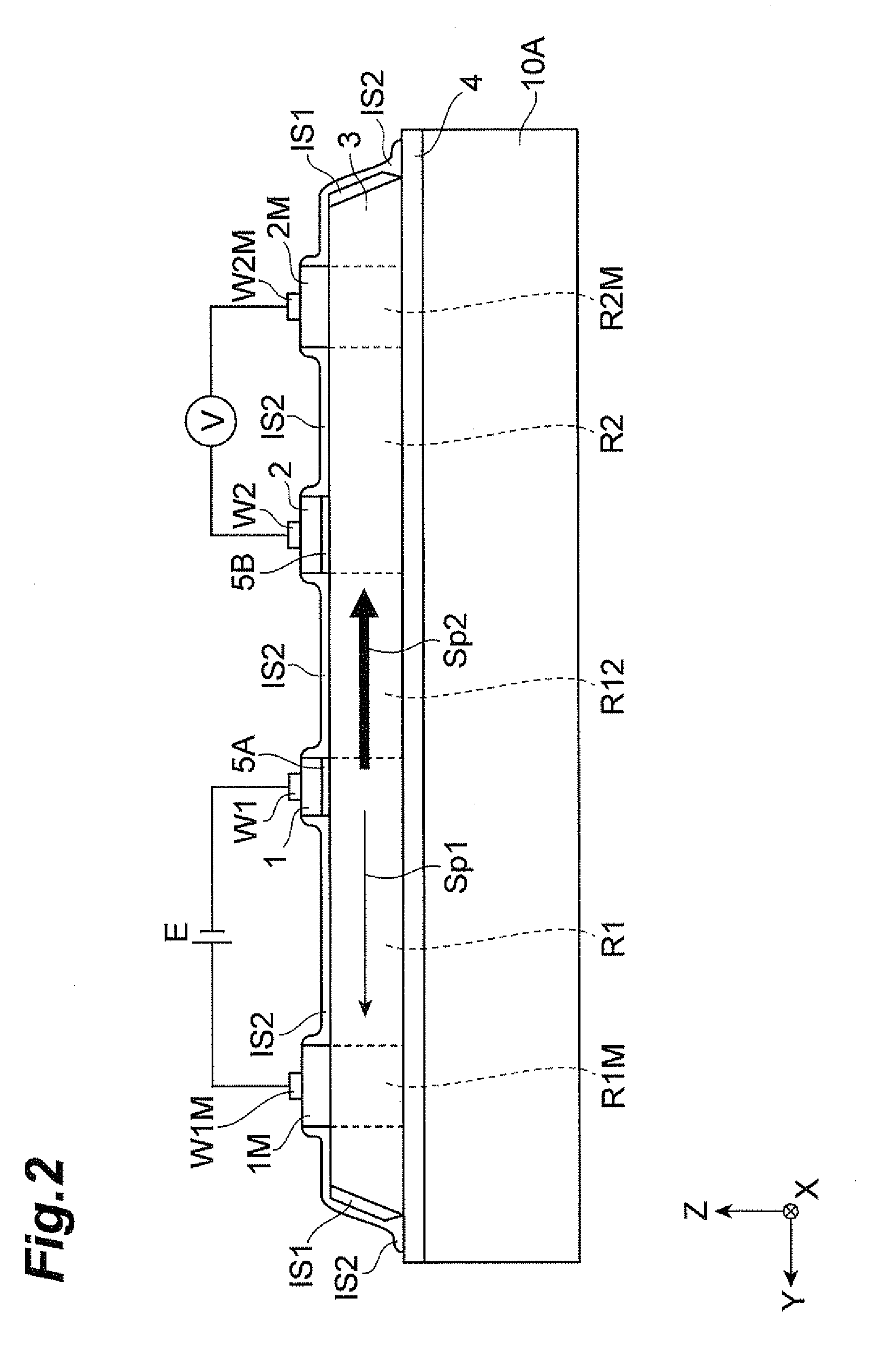
[0045]FIG. 1 is a perspective view of a spin transport device, and FIG. 2 is a view showing a cross-sectional configuration taken along arrow line II-II of the spin transport device shown in FIG. 1.

[0046]An insulating layer 4 (200 nm thick) is provided on a base substrate 10A. A semiconductor layer 3 having a rectangular parallelepiped or tetragonal frustum shape is provided on the insulating layer 4. A longitudinal direction of the semiconductor layer 3 is a Y axis direction in an XYZ three-dimensional Cartesian coordinate system, a transverse direction is an X axis direction, and a thickness direction is a Z axis direction. The semiconductor layer 3 functions as a channel through which spin is transported and diffused. A first ferromagnetic layer 1, a second ferromagnetic layer 2, a firs...


PUM


Abstract

A spin transport device includes a semiconductor layer 3, a first ferromagnetic layer 1 provided on the semiconductor layer 3 via a first tunnel barrier layer 5A, and a second ferromagnetic layer 2 provided on the semiconductor layer 3 via a second tunnel barrier layer 5B to be spaced from the first ferromagnetic layer 1, and the semiconductor layer 3 includes a first region RI broadening in a direction away from the first ferromagnetic layer 1 along a direction orthogonal to a thickness direction from the first ferromagnetic layer 1, and a second region R12 extending in a direction toward the second ferromagnetic layer 2 along the direction orthogonal to the thickness direction from the first ferromagnetic layer 1. The second region R12 has a relatively higher impurity concentration than the first region R1.

Description

BACKGROUND OF THE INVENTION[0001]1. Field of the Invention[0002]The present invention relates to a spin transport device in semiconductor spintronics.[0003]2. Related Background Art[0004]In recent years, a phenomenon of spin transport in a semiconductor, particularly silicon (Si), has attracted much attention. Silicon is a key material in current semiconductor products. If silicon-based spintronics can be realized, new functions can be added to a silicon device without discarding existing technology. An example of such a semiconductor spin transport device includes a spin-MOSFET. Semiconductor spin transport devices include a semiconductor spin transport device using both electric current and spin current (magnetoresistance effect type) and a semiconductor spin transport device using only spin current (non-local structure type).[0005]In the non-local structure type semiconductor spin transport device, since a path of the electric current differs from a path of the spin current, and ...

Claims


Application Information

Patent Timeline
Patent Type & Authority Applications(United States)
IPC IPC(8): H01L29/82
CPCH01L29/0657H01L29/82H01L29/66984
Inventor SASAKI, TOMOYUKIOIKAWA, TOHRU
Owner TDK CORPARATION
Why Eureka
Try Eureka