
Package-on-package semiconductor device

a semiconductor device and packaging technology, applied in semiconductor devices, semiconductor/solid-state device details, electrical equipment, etc., can solve the problems of poor reliability and poor joints of pop semiconductor devices, and achieve the effect of reducing the warpage of the bottom package and strengthening the joints of embedded solder balls

Inactive Publication Date: 2012-10-25
WALTON ADVANCED ENG INC
View PDF7 Cites 39 Cited by
  • Summary
  • Abstract
  • Description
  • Claims
  • Application Information

AI Technical Summary

Benefits of technology

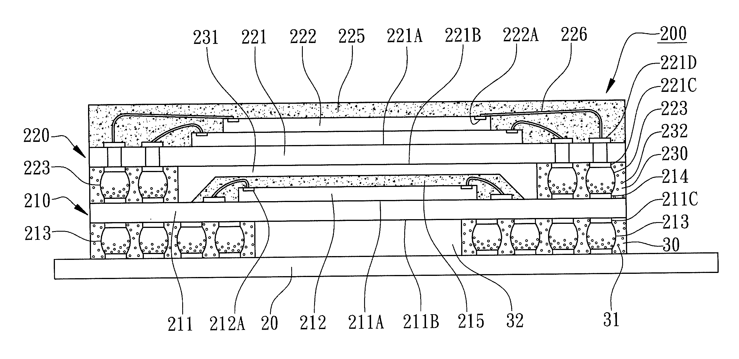
[0005]The main purpose of the present invention is to provide a POP semiconductor device to enhance the joints of embedded solder balls and to effectively reduce substrate warpage of the bottom package to resolve failure of electrical connection due to the breaking of soldering points between the top package and the bottom package.
[0007]The POP semiconductor device according to the present invention has the following advantages and effects:
[0008]1. Through the specific disposition of the ACA layer with a central opening between the top package and the bottom package, the ACA layer adheres the peripheries of the first upper surface of the bottom substrate to the peripheries of the second lower surface of the top substrate and encapsulate the solder balls. In addition to the embedded conductive particles in the solder balls, the joints of the embedded solder balls can greatly be enhanced and the substrate warpage can greatly be reduced to resolve the conventional failure of electrical connection due to the breaking of soldering points between the top package and the bottom package.
[0009]2. Through the partial encapsulation of conductive particles by the solder balls which are further bonded to the ball pads as a technical mean, the joint strength between the solder balls and the ball pads can be reinforced.
[0010]3. Through the encapsulation of solder balls by the ACA layer as a technical mean, the solder balls as the chip interconnections can be encapsulated and protected to avoid environmental contamination.

Problems solved by technology

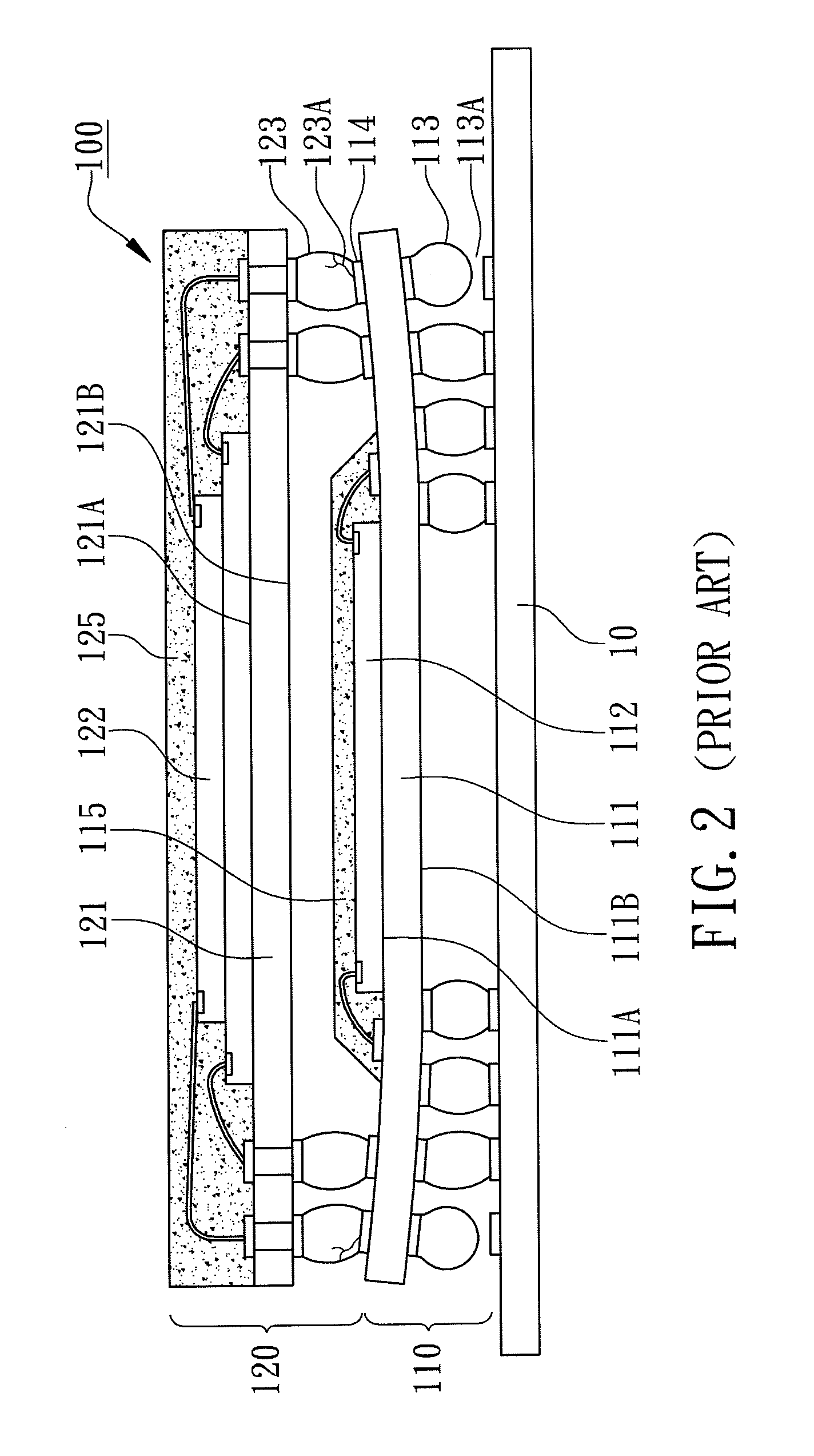
However, temperature of POP semiconductor device 100 rises during thermal cycling test or actual operation, thermal stresses would easily induce in the POP semiconductor device 100 due to the differences of coefficient of thermal expansion (CTE) in different materials in the POP semiconductor device 100, especially easily inducing warpage to the first substrate 111 caused poor joints such as missing solder or cold soldering 113A or breaking of solder balls 123A as shown in FIG. 2 leading to poor reliability of the POP semiconductor device 100.

Method used


Image

  • Package-on-package semiconductor device
  • Package-on-package semiconductor device
  • Package-on-package semiconductor device

Examples


Embodiment Construction

[0019]With reference to the attached drawings, the present invention is described by means of the embodiment(s) below where the attached drawings are simplified for illustration purposes only to illustrate the structures or methods of the present invention by describing the relationships between the components and assembly in the present invention. Therefore, the components shown in the figures are not expressed with the actual numbers, actual shapes, actual dimensions, nor with the actual ratio. Some of the dimensions or dimension ratios have been enlarged or simplified to provide a better illustration. The actual numbers, actual shapes, or actual dimension ratios can be selectively designed and disposed and the detail component layouts may be more complicated.

[0020]According to the first embodiment of the present invention, a POP semiconductor device is revealed in FIG. 3 for a cross-sectional view before assembly and in FIG. 4 for a cross-sectional view after assembly. The POP se...


PUM


Abstract

Disclosed is a package-on-package semiconductor device comprising a bottom package, a top package thereon and a ACA (Anisotropic Conductive Adhesive) layer. A plurality of ball pads are disposed on the peripheries of an upper surface of the substrate of the bottom package. A plurality of solder balls are disposed at the peripheries of the lower surface of the substrate of the top package. The ACA layer having a central opening is interposed between the bottom package and the top package where the ACA layer contains a plurality of conductive particles. Therein, the size of the central opening and the thickness of the ACA layer are selected such that the anisotropic conductive adhesive layer adheres the peripheries of the upper surface of the bottom package to the peripheries of the lower surface of the top package and the solder balls are encapsulated inside the anisotropic conductive adhesive layer. The solder balls encapsulate some of the conductive particles to mechanically joint and electrically connect to the ball pads. Thereby, the bonding strength of the solder balls can be improved and the warpage of the substrate of the bottom package is effectively reduced to avoid failure of electrical connections between both packages caused by the breaking of soldering joints.

Description

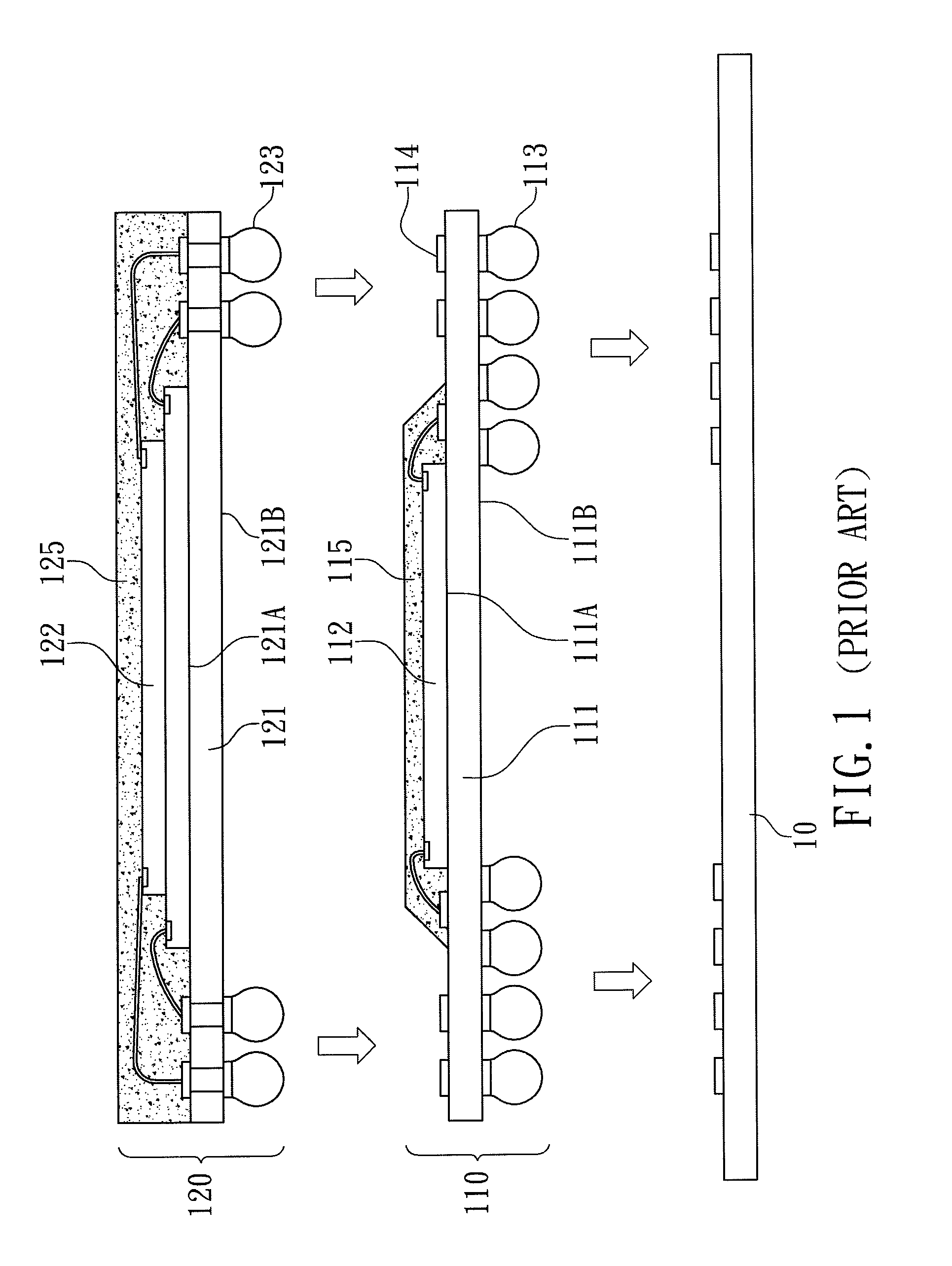
FIELD OF THE INVENTION[0001]The present invention relates to a semiconductor device, and more specifically to a package-on-package semiconductor device.BACKGROUND OF THE INVENTION[0002]Among the modern semiconductor packaging technology, a packaging product formed by stacking two semiconductor packages is developed to meet the requirements of multiple functions with high power within a smaller footprint, i.e., stacked package-on-package (POP) or 3D packages. POP is formed by vertically stacking two or more individual packages together through SMT where the packages have gone through final test (FT) to ensure good packages to form high-density packages with reduced SMT footprint and to avoid the risk of yield loss due to IC fabrication with different functions on a single IC and in a single package. Therefore, POP is an emerging stacked package with mature packaging technology to provide low-cost system-in-package (SIP) solutions, especially suitable for the integration of various co...

Claims


Application Information

Patent Timeline
IPC IPC(8): H01L23/498
CPCH01L2225/0651H01L23/3128H01L2225/1058H01L2225/06568H01L2224/48227H01L2224/48471H01L2924/15311H01L25/105H01L2224/32145H01L2224/32225H01L2224/73265H01L2924/15321H01L2924/3511H01L2225/1023H01L23/562H01L2924/07811H01L2924/00012H01L2924/00H01L24/73
Inventor CHEN, YUNG-HSIANG
Owner WALTON ADVANCED ENG INC
Learn More