Flip chip package for DRAM with two underfill materials

a chip and chip technology, applied in the field of microelectronic packages, can solve the problems of cte stress on the electrical connection between the chip and the higher cte structure of the substrate, and the reliability of conventional microelectronic packages

Active Publication Date: 2014-01-28
INVENSAS CORP
View PDF5 Cites 3 Cited by
  • Summary
  • Abstract
  • Description
  • Claims
  • Application Information

AI Technical Summary

Benefits of technology

[0010]In accordance with an aspect of the invention, a microelectronic package can include a substrate having a first surface and a plurality of substrate contacts at the first surface and a microelectronic element having a front surface and contacts arranged within a contact-bearing region of the front surface. The contacts of the microelectronic element can face the substrate contacts and can be joined thereto. An underfill can be disposed between the substrate first surface and the contact-bearing region of the front surface of the microelectronic element. The underfill can reinforce the joints between the contacts and the substrate contacts. A joining material can bond the substrate first surface with the front surface of the microelectronic element. The joining material can have a Young's modulus less than 75% of a Young's modulus of the underfill.
[0017]Further aspects of the invention can provide systems that incorporate modules and / or components according to the foregoing aspects of the invention, composite chips according to the foregoing aspects of the invention, or both in conjunction with other electronic components electrically connected thereto. In one embodiment, at least one of the other electronic components can be a circuit panel. In an exemplary embodiment, the system can be disposed in and / or mounted to a single housing, which can be a portable housing. In a particular embodiment, a module including a plurality of microelectronic packages as described above can have a circuit panel for transport of signals to and from each of the microelectronic packages. Systems according to preferred embodiments in this aspect of the invention can be more compact than comparable conventional systems.
[0018]In accordance with another aspect of the invention, a method of fabricating a microelectronic package can include the steps of mounting a microelectronic element to a substrate with a joining material, and then forming an underfill between the a first surface of the substrate and a contact-bearing region of a front surface of the microelectronic element. The mounting step can include the step of bonding the front surface of the microelectronic element to the first surface of the substrate with the joining material. The mounting step can also include the step of joining contacts arranged within the contact-bearing region of the front surface of the microelectronic element with corresponding substrate contacts at the substrate first surface. The joining can create electrical contact between the microelectronic element and the substrate. The underfill can reinforce the joints between the contacts and the substrate contacts. The joining material can have a Young's modulus less than 75% of a Young's modulus of the underfill.

Problems solved by technology

Conventional microelectronic packages may have reliability challenges because of a non-optimal stress distribution inside of the package and a mismatch of the coefficient of thermal expansion (CTE) between a semiconductor chip, for example, and the structure to which the chip is bonded.
For example, when the semiconductor chip is bonded to conductive elements of a polymeric substrate, the electrical connections between the chip and the higher CTE structure of the substrate will be under stress due to CTE mismatch.

Method used


Image

  • Flip chip package for DRAM with two underfill materials
  • Flip chip package for DRAM with two underfill materials
  • Flip chip package for DRAM with two underfill materials

Examples


Embodiment Construction

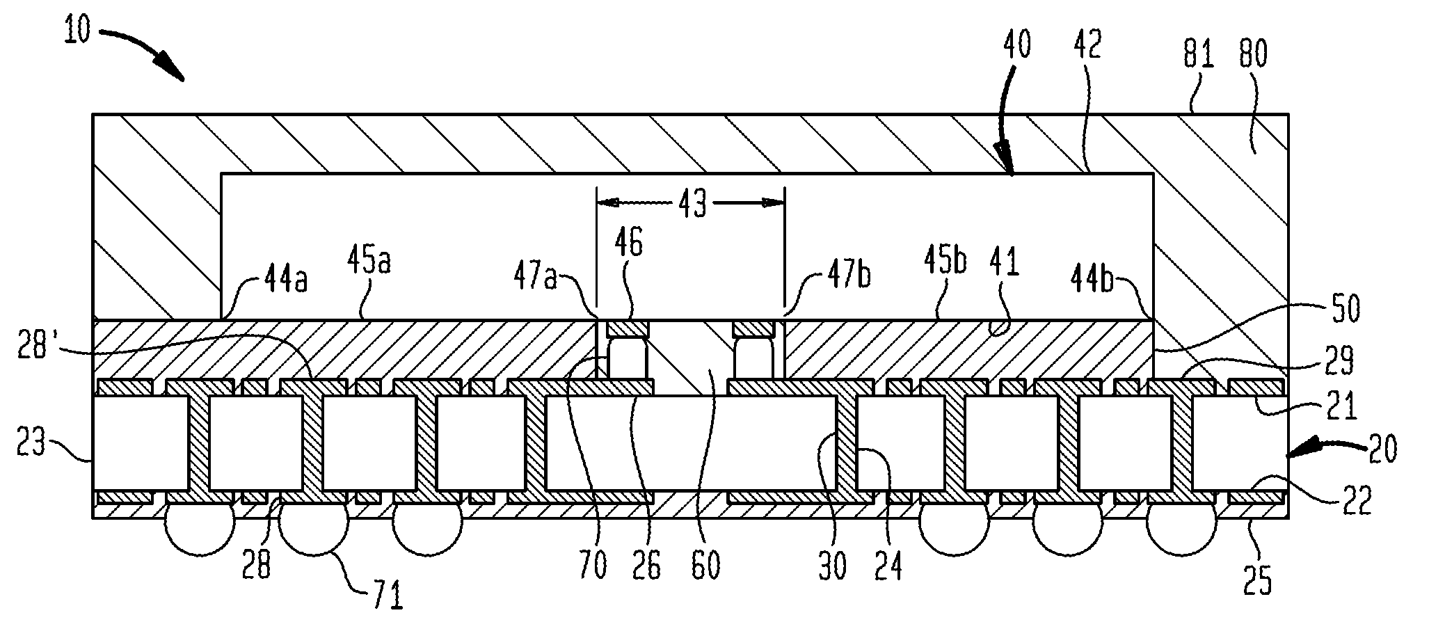
[0028]As illustrated in FIG. 1, a microelectronic package 10 can include a substrate 20 having a first surface 21 and a second surface 22 remote therefrom and a plurality of conductive vias 30 extending therethrough within respective openings 24 between the first and second surfaces. The microelectronic package 10 can also include a microelectronic element 40 that is bonded to the substrate 20 with a joining material 50, an underfill 60 disposed between the substrate 20 and a contact-bearing region 43 of a front surface 41 of the microelectronic element, and an overmold region 80 overlying a rear surface 42 of the microelectronic element and the first surface 21 of the substrate 20.

[0029]The substrate 20 can be partly or entirely made of any suitable dielectric material, such as a polymeric material, or the substrate can be a semiconductor chip, a wafer, or the like. For example, the substrate 20 may comprise a relatively rigid, board-like material such as a thick layer of fiber-rei...


PUM


Abstract

A microelectronic package can include a substrate having a first surface and a plurality of substrate contacts at the first surface and a microelectronic element having a front surface and contacts arranged within a contact-bearing region of the front surface. The contacts of the microelectronic element can face the substrate contacts and can be joined thereto. An underfill can be disposed between the substrate first surface and the contact-bearing region of the front surface of the microelectronic element. The underfill can reinforce the joints between the contacts and the substrate contacts. A joining material can bond the substrate first surface with the front surface of the microelectronic element. The joining material can have a Young's modulus less than 75% of a Young's modulus of the underfill.

Description

BACKGROUND OF THE INVENTION[0001]The present invention relates to microelectronic packages and methods of making such packages, and to components useful in such packages.[0002]Microelectronic elements generally comprise a thin slab of a semiconductor material, such as silicon or gallium arsenide, commonly called a die or a semiconductor chip. Semiconductor chips are commonly provided as individual, prepackaged units. In some unit designs, the semiconductor chip is mounted to a substrate or chip carrier, which is in turn mounted on a circuit panel, such as a printed circuit board.[0003]The active circuitry is fabricated in a first face of the semiconductor chip (e.g., a front surface). To facilitate electrical connection to the active circuitry, the chip is provided with bond pads on the same face. The bond pads are typically placed in a regular array either around the edges of the die or, for many memory devices, in the die center. The bond pads are generally made of a conductive me...

Claims


Application Information

Patent Timeline
Patent Type & Authority Patents(United States)
IPC IPC(8): H01L23/48
CPCH01L23/13H01L2224/33051H01L2224/92125H01L23/49827H01L24/32H01L24/33H01L21/563H01L2224/81801H01L24/81H01L2224/83102H01L2224/9211H01L24/14H01L2924/15311H01L2224/0401H01L24/92H01L2224/33505H01L2224/133H01L2224/1329H01L2224/331H01L2224/73204H01L23/49816H01L2224/14136H01L24/13H01L2224/73203H01L24/16H01L2924/01322H01L2224/16145H01L2224/83192H01L24/29H01L2224/8385H01L2224/05647H01L2224/13111H01L2224/2919H01L2224/16227H01L24/83H01L2224/8184H01L2224/16225H01L2224/131H01L23/3128H01L2224/8185H01L2224/32227H01L24/05H01L2924/07811H01L2224/3303H01L2224/32145H01L24/73H01L2224/29191H01L2924/15151H01L2924/12042H01L2924/181H01L2924/014H01L2924/00014H01L2224/81H01L2224/83H01L2924/00H01L2924/00012H01L2224/32225
Inventor SAKUMA, KAZUOMOHAMMED, ILYASDAMBERG, PHILIP
Owner INVENSAS CORP
Why Eureka
Try Eureka