Chip-type electronic component

Active Publication Date: 2009-12-03
TDK CORPARATION
View PDF7 Cites 4 Cited by
  • Summary
  • Abstract
  • Description
  • Claims
  • Application Information

AI Technical Summary

Benefits of technology

[0009]An object of the present invention is to provide a chip-type electronic component achieving an improvement in joint strength between the terminal electrodes and the ceramic element body, while enhancing design freedom for the arrangement number of internal electrodes.
[0020]Preferably, a length of the third external connection conductor in a direction in which the third internal electrodes and the fourth internal electrodes are opposed (the opposed direction of the third and fourth internal electrodes) is set to be larger than a length of the third terminal electrode in the opposed direction of the third internal electrodes and the fourth internal electrodes, and a length of the fourth external connection conductor in the opposed direction of the third internal electrodes and the fourth internal electrodes is set to be larger than a length of the fourth terminal electrode in the opposed direction of the third internal electrodes and the fourth internal electrodes. In this case, the arrangement number of third and fourth internal electrodes can be increased. Since the lengths of the third and fourth external connection conductors in the opposed direction are relatively long, the contact areas are large between the third and fourth external connection conductors and the ceramic element body. As a consequence, the joint strength is improved between the third and fourth external connection conductors and the ceramic element body.

Problems solved by technology

The size (area) of the terminal electrodes is limited because of design restrictions, e.g., the size (area) of mounting electrodes on the external device side such as a substrate or electronic component on which the chip-type electronic component is to be mounted, and a space to adjacent terminal electrodes.
The internal electrodes cannot be arranged beyond the foregoing range because electrical connection thereof cannot be established with the terminal electrodes; therefore, the number of internal electrodes to be arranged is also limited.
Particularly, in cases where the chip-type electronic component is small in size, the size of the terminal electrodes itself must be small and the arrangement number of internal electrodes (the number of laminated layers thereof) is further limited.
For example, in a case where there is a need for setting of a large capacitance, the arrangement number of internal electrodes needs to be increased, but the arrangement number is limited.
For this reason, it is hard for the chip-type electronic component described in Laid-open No. 02-256216 to meet the need for implementation of large capacitance.
In this case, adhesion deteriorates between the ceramic element body and the terminal electrodes, which could result in degradation of joint strength.

Method used


Image

  • Chip-type electronic component
  • Chip-type electronic component
  • Chip-type electronic component

Examples


Embodiment Construction

[0035]The preferred embodiments of the present invention will be described below in detail with reference to the accompanying drawings. In the description, the same elements or elements with the same functionality will be denoted by the same reference symbols, without redundant description.

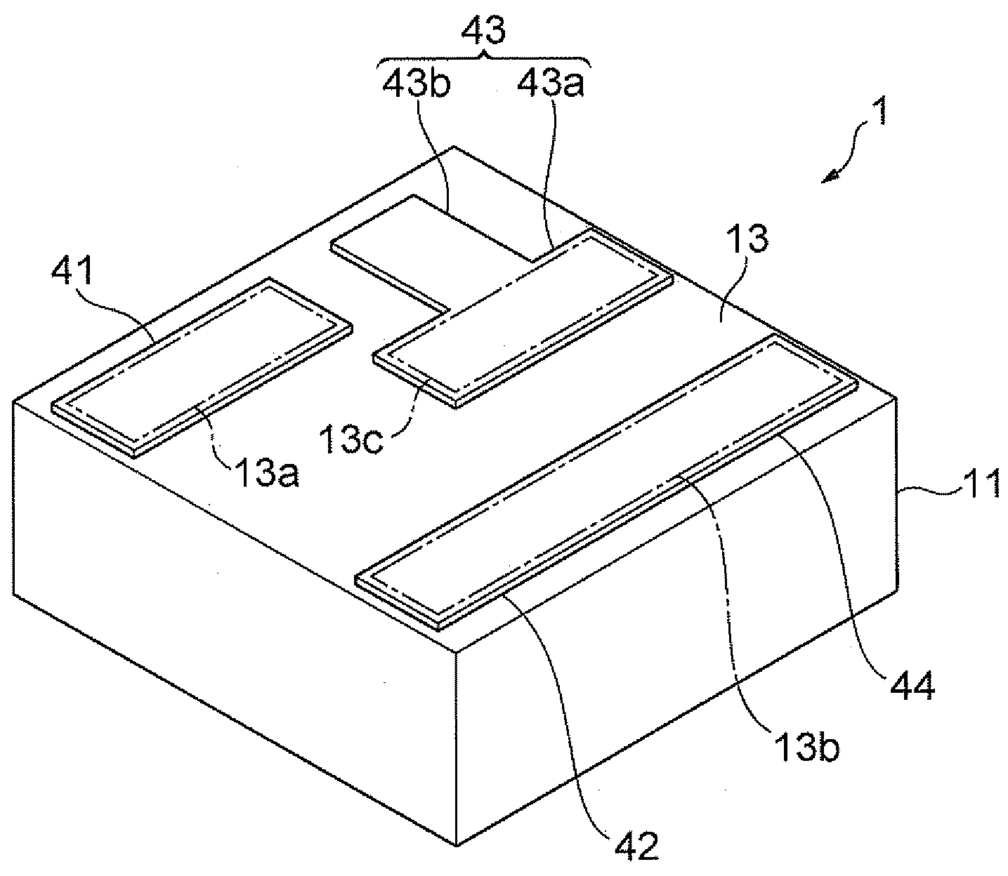
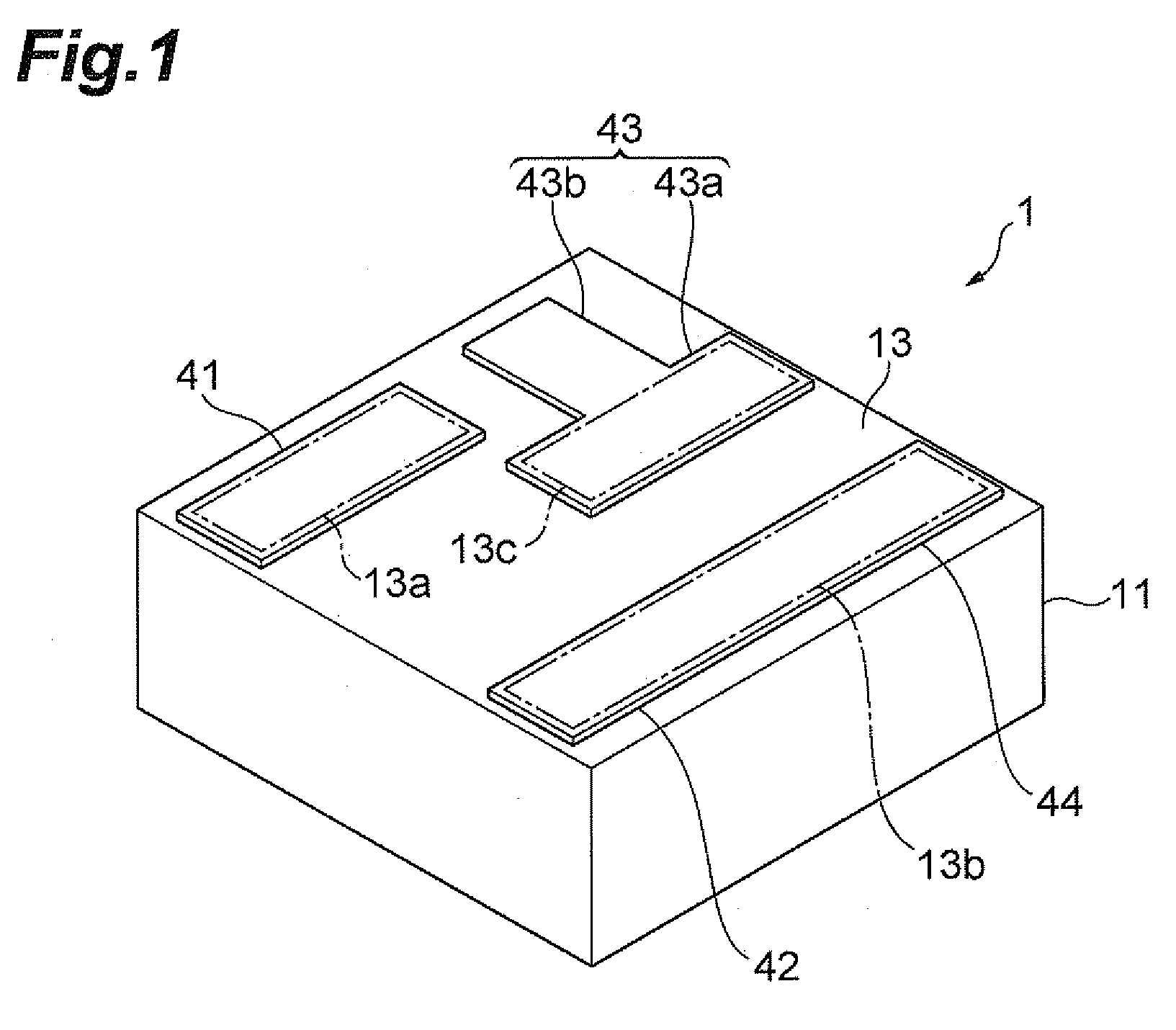
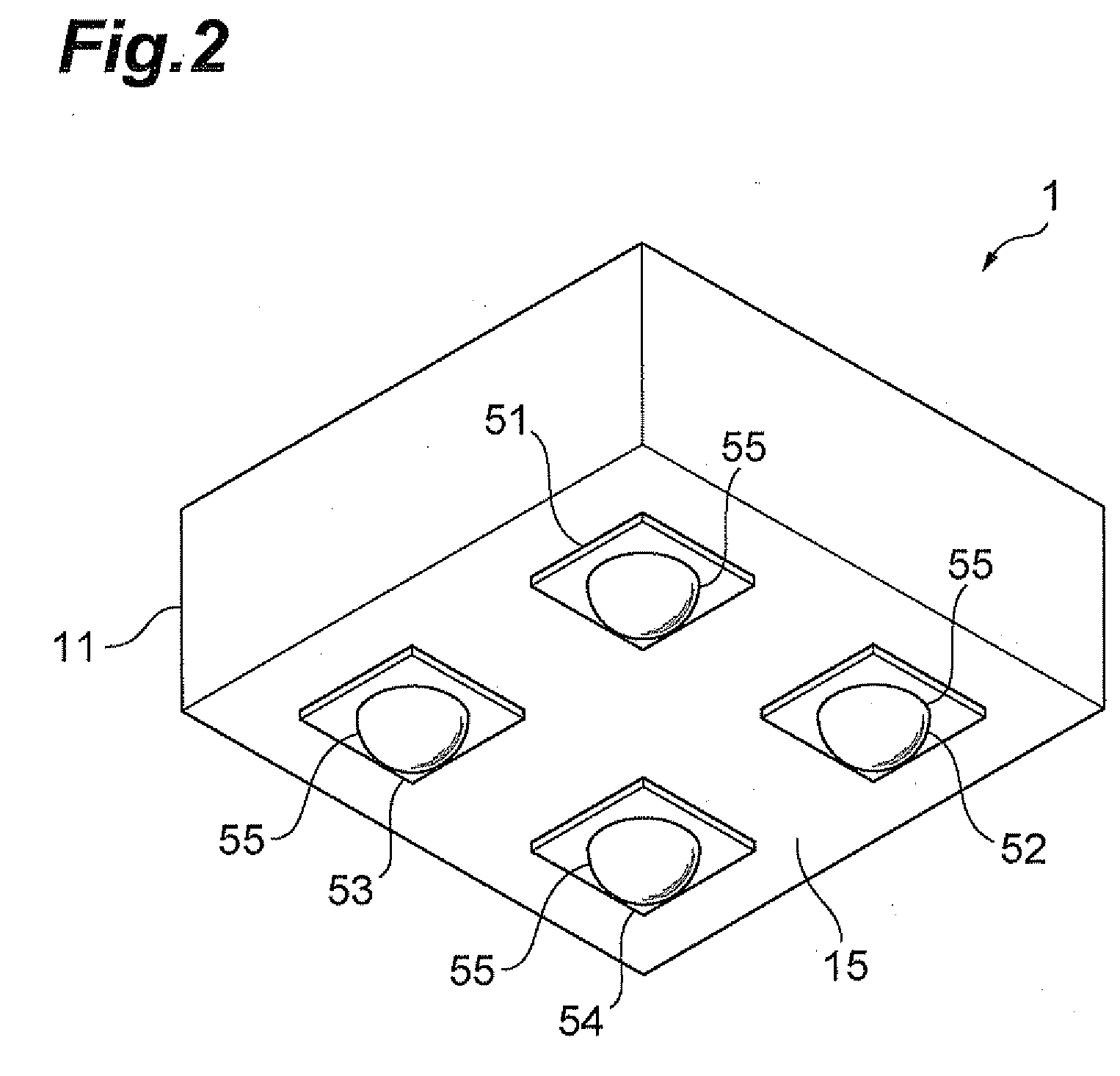
[0036]FIG. 1 and FIG. 2 are perspective views showing a configuration of a multilayer chip varistor according to an embodiment of the present invention. FIG. 3 is an exploded perspective view of a varistor element body included in the multilayer chip varistor of the first embodiment. FIGS. 4A to AE are drawings showing configurations of first and second internal electrodes and first and second internal connection conductors. FIGS. 5 to 7 are drawings for explaining sectional configurations of the multilayer chip varistor of the embodiment.

[0037]The multilayer chip varistor 1 of the present embodiment is a varistor element of a so-called BGA (Ball Grid Array) package-compatible type, which is to be...


PUM

PropertyMeasurementUnit
Lengthaaaaaaaaaa

Abstract

A chip-type electronic component has: a ceramic element body; a plurality of first and second internal electrodes arranged in the ceramic element body so as to be opposed at least in part to each other; a first external connection conductor to which the plurality of first internal electrodes are connected; a second external connection conductor to which the plurality of second internal electrodes are connected; first and second terminal electrodes; a first internal connection conductor arranged in the ceramic element body and connecting the first external connection conductor and the first terminal electrode; and a second internal connection conductor arranged in the ceramic element body and connecting the second external connection conductor and the second terminal electrode. The number of the first internal connection conductor is set to be smaller than the number of the first internal electrodes and the number of the second internal connection conductor is set to be smaller than the number of the second internal electrodes.

Description

BACKGROUND OF THE INVENTION[0001]1. Field of the Invention[0002]The present invention relates to a chip-type electronic component.[0003]2. Related Background Art[0004]There is a known chip-type electronic component which has a ceramic element body consisting of a plurality of ceramic layers laminated together, a plurality of first and second internal electrodes arranged alternately in the ceramic element body so as to be opposed at least in part to each other, a first terminal electrode which is arranged on an external surface of the ceramic element body and to which the plurality of first internal electrodes are connected, and a second terminal electrode which is arranged on the external surface of the ceramic element body and to which the plurality of second internal electrodes are connected (e.g., cf. Japanese Patent Application Laid-open No. 02-256216).SUMMARY OF THE INVENTION[0005]Since in the chip-type electronic component described in Laid-open No. 02-256216 the plurality of ...

Claims


Application Information

Patent Timeline
IPC IPC(8): H01G4/228H01C7/10H01C1/142
CPCH01C1/142H01C7/10H01G4/30H01G4/12H01G4/228H01G4/005
Inventor UEDA, KANAMEMATSUOKA, DAICHIDA, NAOKISOMA, IZURUSAITO, HISAYOSHIMORIAI, KATSUNARI
Owner TDK CORPARATION
Why Eureka
Try Eureka