Liquid crystal display device

a liquid crystal display and display device technology, applied in non-linear optics, instruments, optics, etc., can solve the problems of liquid crystal display devices with a problem, the orientation control cannot be applied to liquid crystal, and the satisfactory rubbing orientation process cannot be applied, so as to enhance the transmissivity of a pixel, reduce the area of a shading film, and enhance the effect of a high luminance screen

Active Publication Date: 2012-10-25
JAPAN DISPLAY INC
View PDF6 Cites 19 Cited by
  • Summary
  • Abstract
  • Description
  • Claims
  • Application Information

AI Technical Summary

Benefits of technology

[0008]An object of the present invention is to possibly reduce the area of a shading film in a contact hole, to en

Problems solved by technology

In the meantime, the liquid crystal display device has a problem related to an angle of visibility.
However, since the contact hole is concave, a satisfactory rubbing orientation process cannot be applied to the alignment film in this part and orientation control cannot be applied to liquid crystal.
Accordingly, in the

Method used


Image

  • Liquid crystal display device
  • Liquid crystal display device
  • Liquid crystal display device

Examples


first embodiment

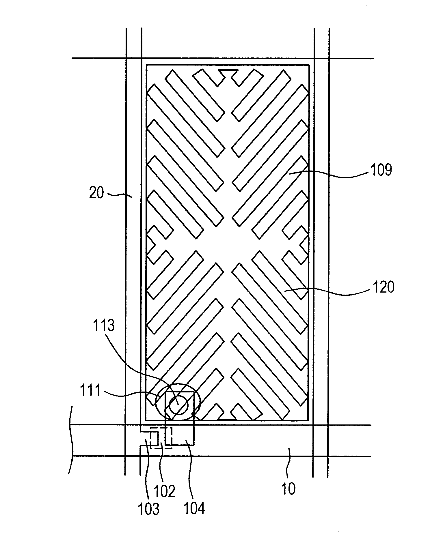
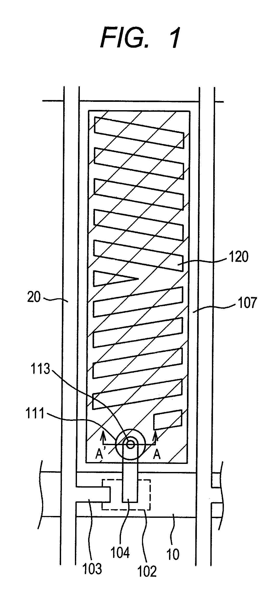
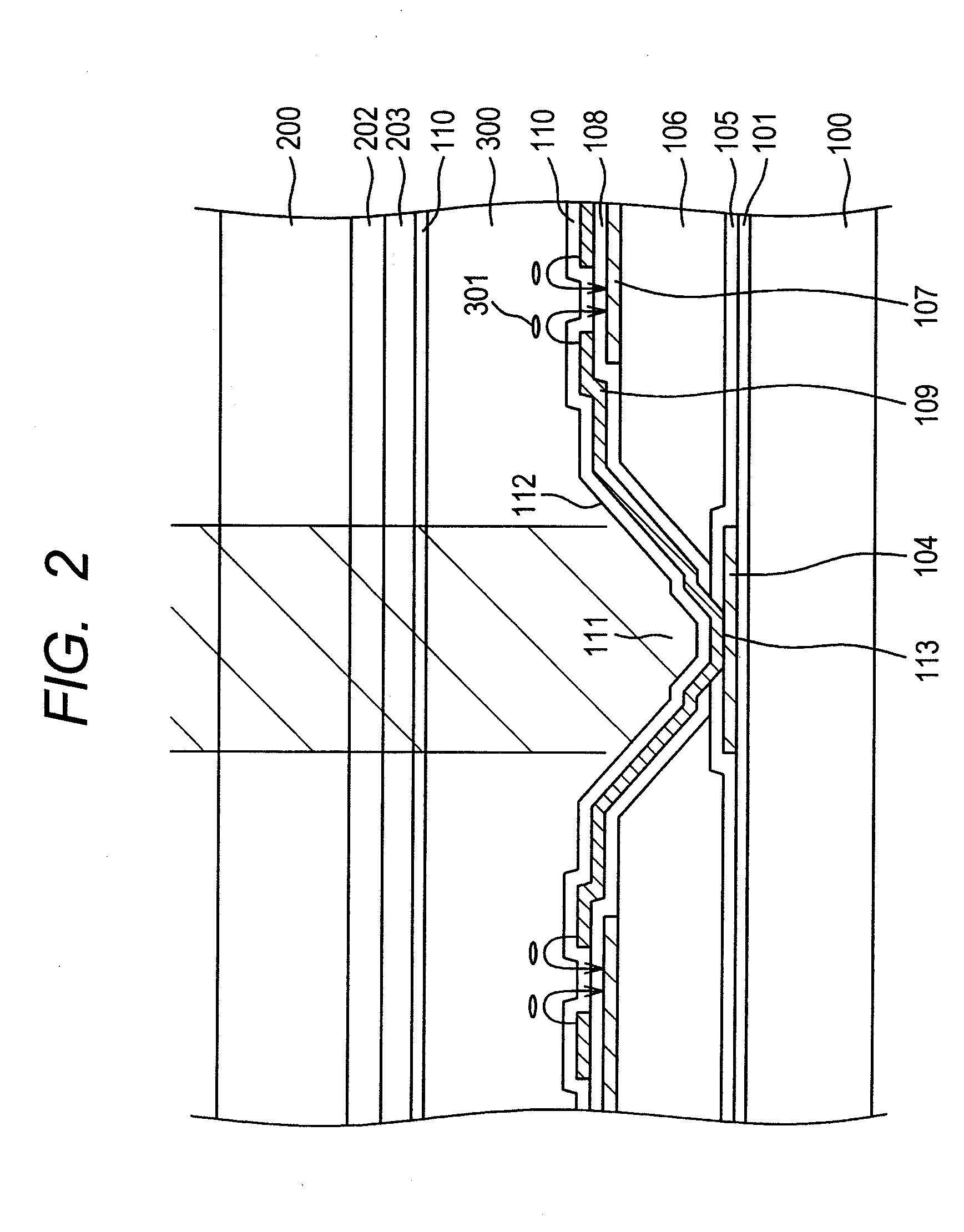
[0033]A first embodiment relates to IPS having configuration that a flat solid counter electrode 107 is arranged on the downside and a pixel electrode 109 having a slit 120 is arranged on the upside via an interlayer insulation film 108. FIG. 1 shows the planar configuration of pixels in this embodiment and FIG. 2 is a sectional view viewed along a line A-A′ in FIG. 1. In FIGS. 1 and 2, an alignment film 110 controls orientation depending upon optical orientation. FIG. 3 is a plan showing pixels in the related art having the same electrode configuration and FIG. 4 is a sectional view viewed along a line B-B′ in FIG. 3. In the related art shown in FIGS. 3 and 4, an alignment film 110 controls orientation depending upon rubbing.

[0034]To explain characteristics of the present invention, FIGS. 3 and 4 showing a configuration in the related art will be first described. In FIG. 3, a pixel area is formed in an area enclosed by a picture signal conductor 20 vertically extended and a scannin...

second embodiment

[0051]In a second embodiment, the present invention is applied to IPS having configuration that a flat and solid pixel electrode 109 is arranged on the downside and a counter electrode 107 having a slit 120 is arranged on the upside via an interlayer insulation film 108 reversely to the first embodiment. FIG. 5 shows a planar configuration of a pixel in this embodiment and FIG. 6 is a sectional view viewed along a line C-C′ in FIG. 5. In FIGS. 5 and 6 showing this embodiment, an alignment film 110 also controls orientation depending upon optical orientation. FIG. 7 is a plan showing a pixel in the related art having the same electrode configuration and FIG. 8 is a sectional view viewed along a line D-D′ in FIG. 7. In the related art shown in FIGS. 7 and 8, an alignment film 110 controls orientation depending upon rubbing.

[0052]To explain the characteristics of the present invention, FIGS. 7 and 8 showing configuration in the related art will be first described. FIG. 7 is similar to ...

third embodiment

[0065]In a third embodiment, as in the second embodiment, the present invention is also applied to IPS having a configuration that a flat and solid pixel electrode 109 is arranged on the downside and a counter electrode 107 having a slit 120 is arranged on the upside via an interlayer insulation film 108. FIG. 9 shows the planar configuration of a pixel in this embodiment and FIG. 10 is a sectional view viewed along a line E-E′ in FIG. 9. In FIGS. 9 and 10 showing this embodiment, an alignment film 110 also controls orientation depending upon optical orientation. FIG. 11 is a plan showing a pixel in the related art having the similar electrode configuration and FIG. 12 is a sectional view viewed along a line F-F′ in FIG. 11. In the related art shown in FIGS. 11 and 12, an alignment film 110 controls orientation depending upon rubbing.

[0066]To explain the characteristics of the present invention, FIGS. 11 and 12 showing the related art will be first described. FIG. 11 is significantl...


PUM


Abstract

An object of the present invention is to enhance transmissivity and the luminance of a screen in an IPS liquid crystal display device. To achieve the object, in the IPS liquid crystal display device according to the present invention, a counter electrode is formed flatly and solidly on an organic passivation film, a pixel electrode having a slit is formed on the counter electrode via an interlayer insulation film, and an alignment film the orientation of which is controlled by optical orientation is formed on the pixel electrode. The transmissivity is enhanced by also making the inside of the contact hole function as a transmissible area for image formation by applying optical orientation to the alignment film in the contact hole to result in enhancement of the luminance of the screen.

Description

CLAIM OF PRIORITY[0001]The present application claims priority from Japanese Patent Application JP 2011-095969 filed on Apr. 22, 2011, the content of which is hereby incorporated by reference into this application.FIELD OF THE INVENTION[0002]The present invention relates to a liquid crystal display device, and particularly relates to a liquid crystal display device where luminance is enhanced by providing an orientation control function to an alignment film by the irradiation of light and enhancing transmissivity in a pixel.BACKGROUND OF THE INVENTION[0003]In a liquid crystal display device, a thin film transistor (TFT) substrate on which a pixel electrode and a thin film transistor (TFT) and others are formed in a matrix and a counter substrate on which a color filter and others are formed in a location corresponding to the pixel electrode of the TFT substrate opposite to the TFT substrate are installed, and liquid crystal is held between the TFT substrate and the counter substrate...

Claims


Application Information

Patent Timeline
IPC IPC(8): G02F1/136
CPCG02F1/133707G02F1/134336G02F1/134309G02F1/1343G02F1/1337G02F1/1368G02F1/136227
Inventor TOMIOKA, YASUSHIKUNIMATSU, NOBORUSATO, TAKESHIMATSUMORI, MASAKI
Owner JAPAN DISPLAY INC
Why Eureka
Try Eureka