Atomic layer deposition of metal phosphates and lithium silicates

a technology of metal phosphate and lithium silicate, which is applied in the direction of chemical vapor deposition coating, coating, plasma technique, etc., can solve the problems of difficult 3d battery manufacturing, limited development of ald-grown phosphate thin film process, and high cost of lithium in the film. , to achieve the effect of increasing the amount of lithium in the film

Active Publication Date: 2012-11-01
ASM IP HLDG BV
View PDF6 Cites 31 Cited by
  • Summary
  • Abstract
  • Description
  • Claims
  • Application Information

AI Technical Summary

Benefits of technology

[0031]In some embodiments, additional ALD cycles can be included to adjust the composition of the lithium silicate. For example, in some embodiments one or more lithium oxide deposition cycles are included. These additional lithium oxide deposition cycles may increase the amount of lithium in the film. In some embodiments the additional cycles comprise alternately and sequentially contacting the substrate with a lithium precursor, such as lithium tert-butoxide, and on oxygen precursor, such as water.
[0032]In some embodiments a different metal is incorporated into the film, such as aluminum, by including a different metal oxide deposition cycle. For example, one or more aluminum oxide deposition cycles may be incorporated to form lithium aluminum silicate. An aluminum oxide deposition cycle may comprise alternately and sequentially contacting the substrate with an aluminum precursor, such as trimethylaluminum (TMA) and an oxygen precursor, such as ozone. The stoichiometry of the LixAlySizO that is deposited can be varied, by varying the ratio of lithium silicate and aluminum oxide deposition cycles. In some embodiments, LiAlSiO4 is deposited

Problems solved by technology

Fabrication of 3D batteries is challenging because all of the materials, including electrodes, barriers and electrolyte, have to be made conformally.
Mixed metal phosphates can be very demanding to manufacture with precision.
While ALD has been a reliable technique to deposit complex materials homogeneously over large areas and on demanding, complex structures, the development of ALD-grown phosphate thin film processes has been quite limited and only a few metal phosphate thin film processes have been reported.
The use of ALD for phosphate thin film deposition has been quite scarce.
This kind of approach may result in long and complicated growth cycles, which increases the total deposition time required.

Method used


Image

  • Atomic layer deposition of metal phosphates and lithium silicates
  • Atomic layer deposition of metal phosphates and lithium silicates
  • Atomic layer deposition of metal phosphates and lithium silicates

Examples


examples

ALD of Titanium and Aluminum Phosphates

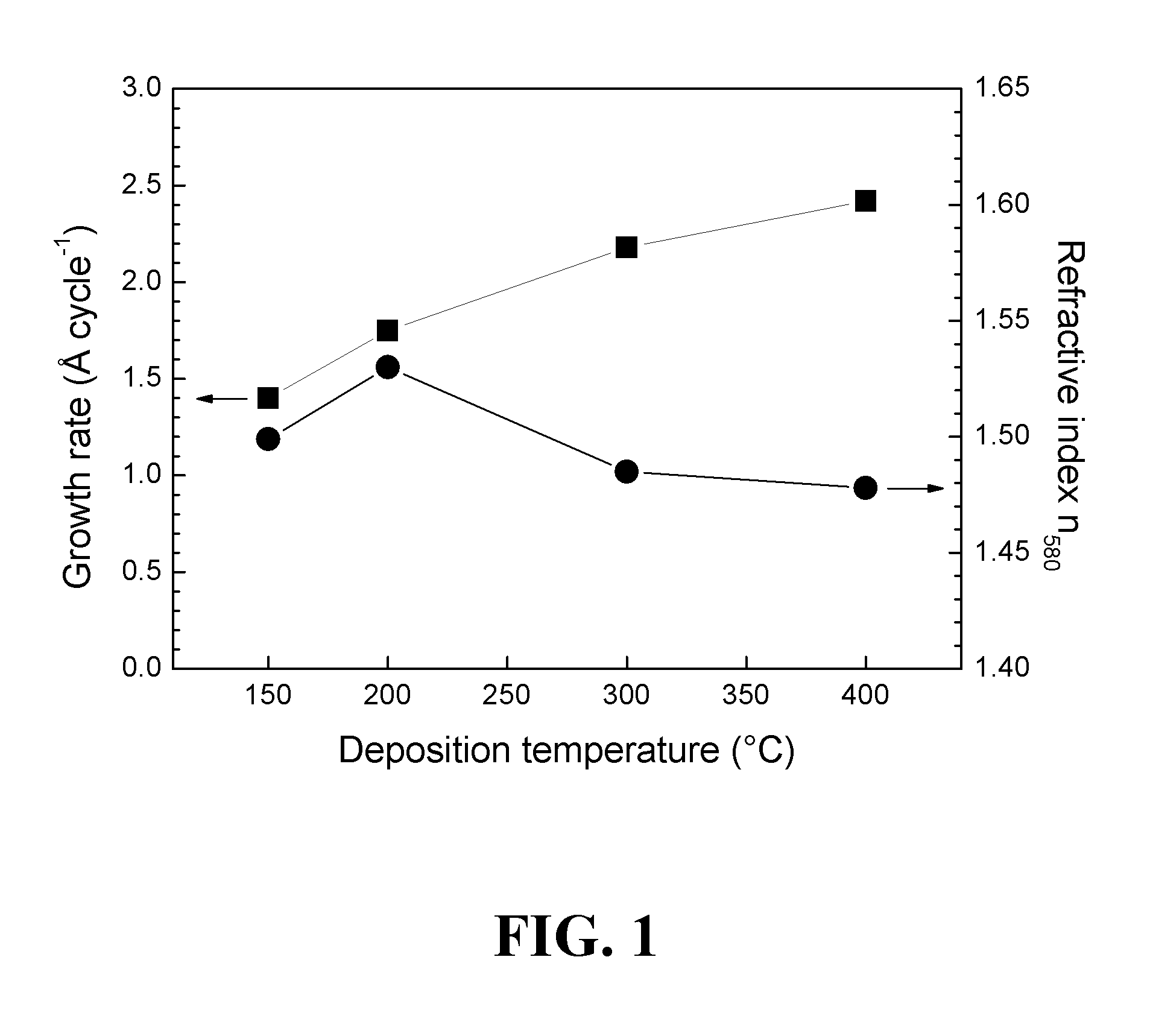
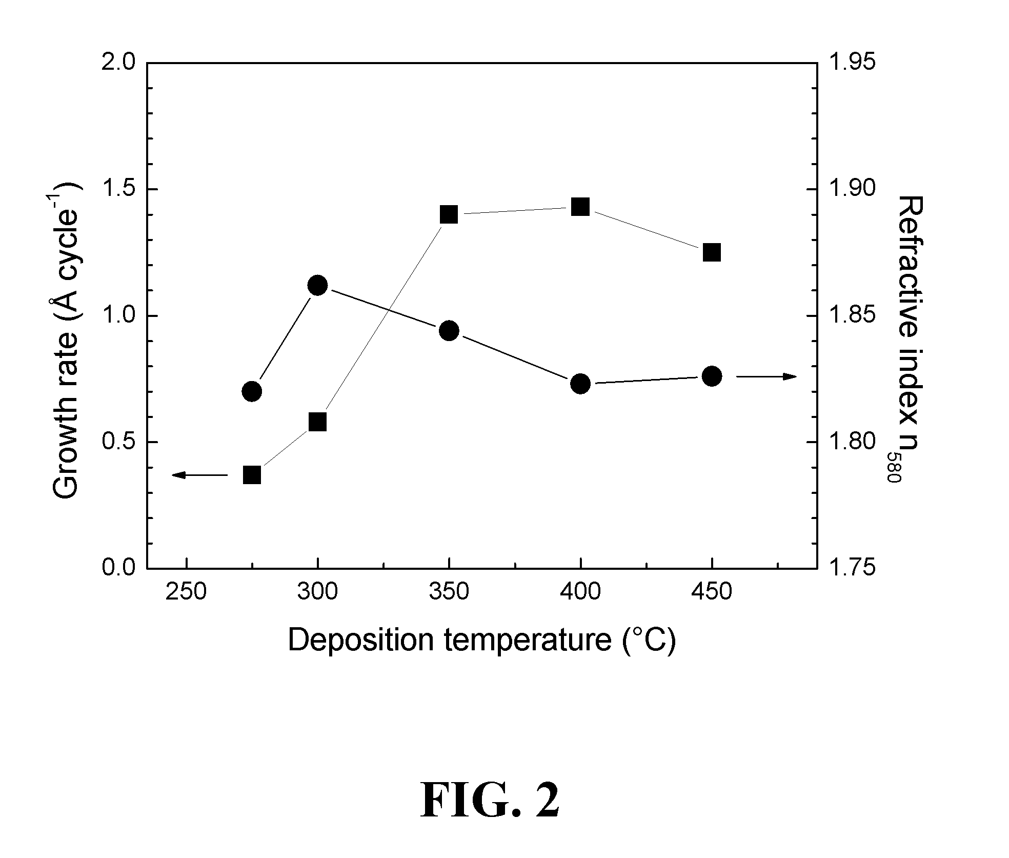
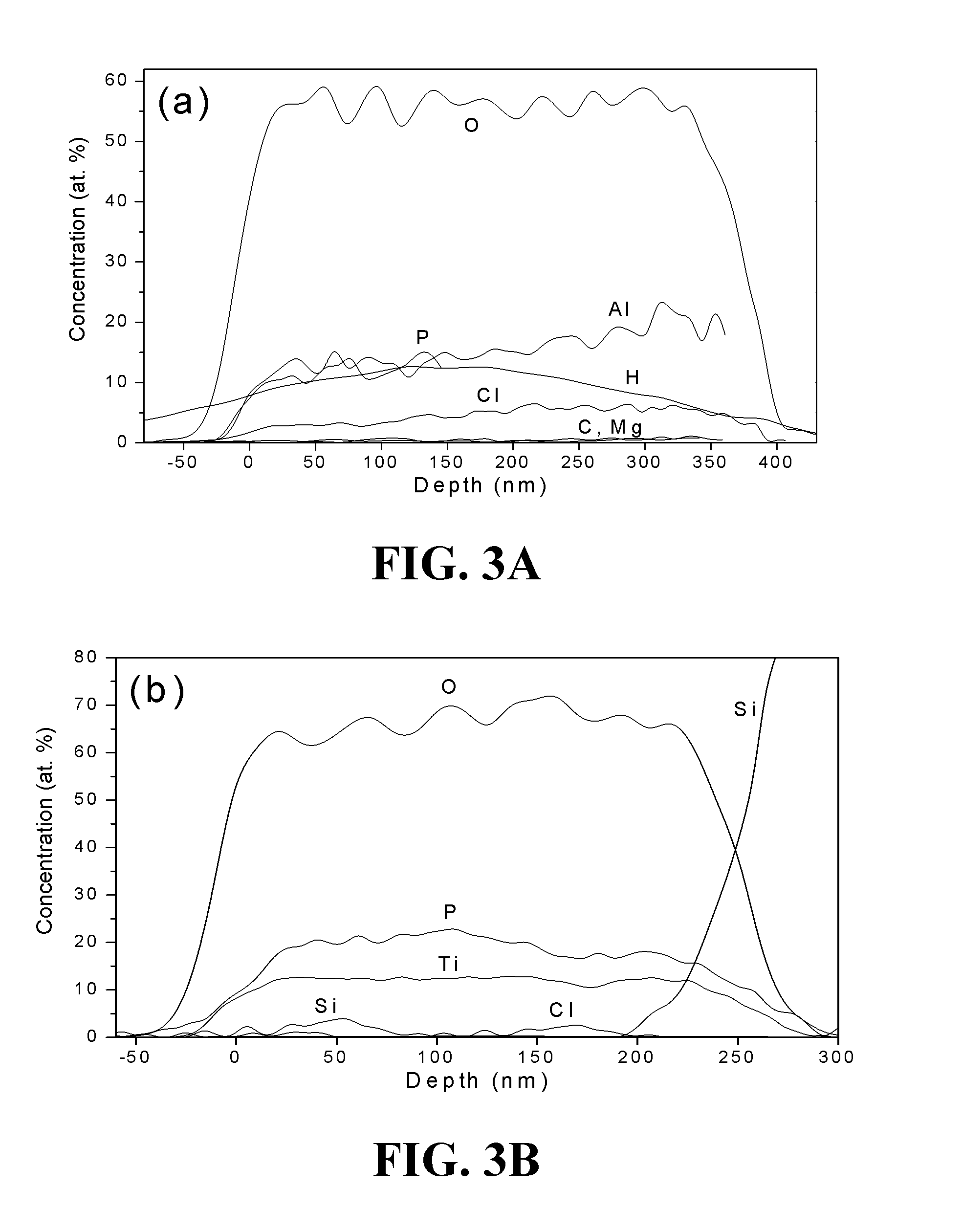
[0126]The atomic layer deposition (ALD) of phosphate containing thin films using reactions between metal halide and phosphorus source without any additional oxygen sources was examined. Two very common metal halides, AlCl3 and TiCl4, were used in conjunction with trimethyl phosphate (TMPO) to grow corresponding metal phosphate films. Aluminum phosphate thin films were deposited at temperatures between 150 and 400° C. while titanium phosphate films grew between 275 and 450° C. Amorphous films of Al2.6PO7.0 and Al1.6PO5.6 were deposited at 200 and 300° C., respectively, while the amorphous titanium phosphate films deposited at 300 and 400° C. consisted of Ti0.8PO3.9 and Ti0.6PO3.5 (Ti1.2P2O7). The films were analyzed using high temperature XRD to study the crystallization and stability of the deposited films. Also the surface morphology of the annealed films was examined by FESEM.

[0127]Thin films were grown in a cross-flow F-120 ALD reactor (ASM ...


PUM

PropertyMeasurementUnit
temperatureaaaaaaaaaa

Abstract

The present application relates to atomic layer deposition (ALD) processes for producing metal phosphates such as titanium phosphate, aluminum phosphate and lithium phosphate, as well as to ALD processes for depositing lithium silicates.

Description

REFERENCE TO RELATED APPLICATIONS[0001]The present application claims priority to U.S. Provisional Application No. 61 / 469,530, filed Mar. 30, 2011, the disclosure of which is hereby incorporated by reference in its entirety.BACKGROUND OF THE INVENTION[0002]1. Field of the Invention[0003]The present application relates to atomic layer deposition of metal compounds that find use, for example, in lithium ion battery applications.[0004]2. Description of the Related Art[0005]Atomic layer deposition (ALD) of lithium-containing compounds has recently received attention due in large part to the need for conformal materials in Li ion batteries used in electronic devices. For safety reasons, all-solid-state batteries are of great interest. The power density of all-solid-state batteries can be improved by moving from planar to three-dimensional structures. Fabrication of 3D batteries is challenging because all of the materials, including electrodes, barriers and electrolyte, have to be made co...

Claims


Application Information

Patent Timeline
Patent Type & Authority Applications(United States)
IPC IPC(8): C23C16/06C23C16/50
CPCC23C16/08C23C16/50C23C16/30C23C16/18C23C16/401C23C16/45527
Inventor HAMALAINEN, JANIHOLOPAINEN, JANIHATANPAA, TIMORITALA, MIKKOLESKELA, MARKKU
Owner ASM IP HLDG BV
Why Eureka
Try Eureka