Seebeck/peltier thermoelectric conversion device employing a stack of alternated nanometric layers of conductive and dielectric material and fabrication process

a technology of dielectric material and thermoelectric conversion device, which is applied in the direction of thermoelectric device junction materials, thermoelectric device manufacture/treatment, electrical apparatus, etc., can solve the problems of silicon nanowire devices being made with techniques unsuitable for industrialization on a large scale, and achieve the effect of relieving mechanical stresses

Inactive Publication Date: 2012-11-08
CONSORZIO DELTA TI RES
View PDF4 Cites 0 Cited by
  • Summary
  • Abstract
  • Description
  • Claims
  • Application Information

AI Technical Summary

Benefits of technology

[0035]The final pyrolitic treatment for converting the sub-stoichiometric oxide film to a population of dielectric clusters of stoichiometric oxide relieves mechanical stresses intrinsic to the stacking of alternately deposited layers of different materials. Moreover, such a deliberate loss of electrical insulation among the stacked conductive nanolayers of deposited metallic or semiconductor material avoids possible unbalances of internal electrical resistance across the septum and attendant power losses that may arise with a layered stack of alternated, uninterrupted layers of conductive and of dielectric material. At the same time, substantial confinement of migrating phonons in the conductive layers alternated to the dielectric oxide-rich layers is retained.

Problems solved by technology

Unfortunately, these test devices made with silicon nanowires are made with techniques unsuitable to industrialization on large scale.

Method used


Image

  • Seebeck/peltier thermoelectric conversion device employing a stack of alternated nanometric layers of conductive and dielectric material and fabrication process
  • Seebeck/peltier thermoelectric conversion device employing a stack of alternated nanometric layers of conductive and dielectric material and fabrication process
  • Seebeck/peltier thermoelectric conversion device employing a stack of alternated nanometric layers of conductive and dielectric material and fabrication process

Examples


Embodiment Construction

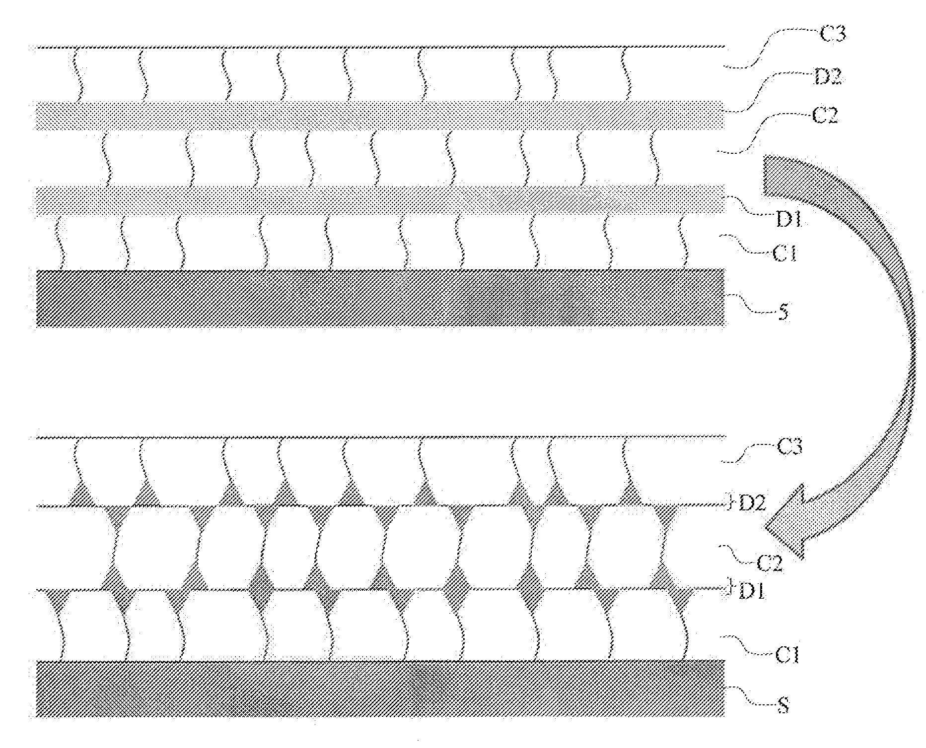
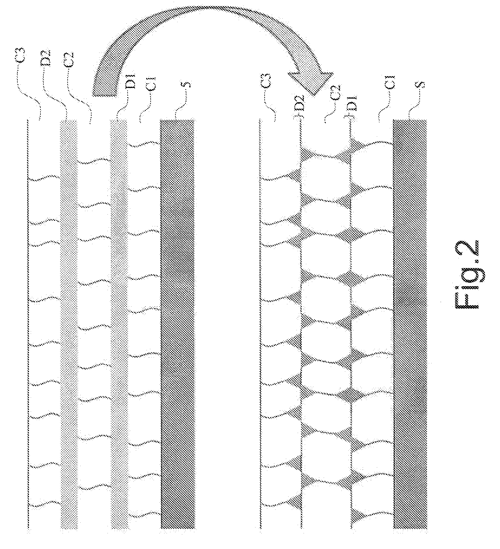
[0041]The exemplary embodiments presented herein below have an exclusively illustrative purpose and are not intended to limit the invention that can be practiced by any expert of the field even by modifying the deposition-oxidation processes or use different conductive or semiconducting materials and different dielectric materials.

[0042]Referring to FIG. 1, in building a multilayered stack of this invention, one may start depositing a first electrical conductive layer of doped silicon C1 of nanometric thickness over a substantially flat dielectric substrate S, for example a planar glass sheet, by vapor phase (CVD or LP-CVD) feeding in an low-pressure, heated deposition chamber silane (SiH4) and a suitable dopant compound such as PH3, AsH3 or B2H6, diluted in N2, at a temperature in the range of 600-800° C.

[0043]Such a first nanometric layer C1 doped silicon semiconductor may have a substantially uniform thickness of about 40-50 nm with little or no surface roughness.

[0044]Thereafter...


PUM

PropertyMeasurementUnit
thicknessaaaaaaaaaa
thicknessaaaaaaaaaa
thicknessaaaaaaaaaa

Abstract

A multilayered stack useful for constituting a Seebeck-Peltier effect electrically conductive septum with opposite hot-side and cold-side metallizations for connection to an electrical circuit, comprises a stacked succession of layers (Ci) of electrically conductive material alternated to dielectric oxide layers (Di) in form of a continuous film or of densely dispersed nano and sub-nano particles or clusters of particles of oxide; at least the electrically conductive layers having mean thickness ranging from 5 to 100 nm and surface irregularities at the interfaces with the dielectric oxide layers of mean peak-to-valley amplitude and mean periodicity comprised between 5 to 20 nm.Various processes adapted to build a multilayered stack of these characteristics are described.

Description

BACKGROUND[0001]1. Technical Field[0002]The disclosure relates in general to Seebeck / Peltier effect thermoelectric conversion devices and in particular to devices using layers of conductive or semi conductive material deposited over a substrate even of large size by common planar techniques and with electrical contacts definable with noncritical lithographic or serigraphic techniques.[0003]2. Reference Notions[0004]The Seebeck effect is a thermoelectric phenomenon according to which a difference of temperature at the opposite ends of an elongated conductor or semiconductor generates electricity. The effect, discovered by the physicist Thomas J. Seebeck in 1821, manifests itself with the presence of a voltage difference at the two ends of a conductive bar subjected to a gradient of temperature ∇T. In a circuit including two junctions kept at different temperatures T1 and T2, between different materials A and B the voltage difference between the two junctions is given by:V=∫T1T2[SB(T)...

Claims


Application Information

Patent Timeline
Patent Type & Authority Applications(United States)
IPC IPC(8): H01L35/28H01L35/14
CPCH01L35/34H01L35/32H10N10/01H10N10/17
Inventor NARDUCCI, DARIOCEROFOLINI, GIANFRANCOLONATI, ELENA
Owner CONSORZIO DELTA TI RES
Why Eureka
Try Eureka