Semiconductor storage device

a technology of semiconductor devices and storage devices, applied in semiconductor devices, digital storage, instruments, etc., can solve the problems of erroneous write operation, need a long current application time, and inability to store information in unselected cells, etc., to achieve high integration, high reliability, and large capacity

Inactive Publication Date: 2012-11-15
HITACHI LTD
View PDF4 Cites 37 Cited by
  • Summary
  • Abstract
  • Description
  • Claims
  • Application Information

AI Technical Summary

Benefits of technology

[0005]Owing to a progress of photo-lithography, a memory array disclosed by Japanese Unexamined Patent Application Publication No. 2008-160004 is capable of reducing the bottom area of a structure formed at points where the word line WL, the bit line BL and the source line SL intersect with each other. In concert with this, it is desirable to suppress the aspect ratio of the interconnect hole by reducing a length in a direction vertical to the semiconductor substrate in order to facilitate a three-dimensional process.
[0007]The present invention is provided to address such problems mentioned above. It is an object of the present invention to suppress the possibility of an erroneous write operation in a semiconductor storage device adopting a phase-change memory which stores information by utilizing the Joule heat.
[0009]According to an aspect of the present invention, it is possible to achieve a semiconductor storage device which adopts a large capacity phase-change memory of high integration and high reliability.

Problems solved by technology

However, if an interval between upper and lower memory cells becomes narrower, there is a concern that all memory cells in the structure mentioned above may be heated up to a crystallization temperature during a set operation (here, crystallization of the phase-change element) which needs a long current application time.
This means that storage information in unselected cells may be reversed by error and thereby an erroneous write operation occurs.

Method used


Image

  • Semiconductor storage device
  • Semiconductor storage device
  • Semiconductor storage device

Examples


first embodiment

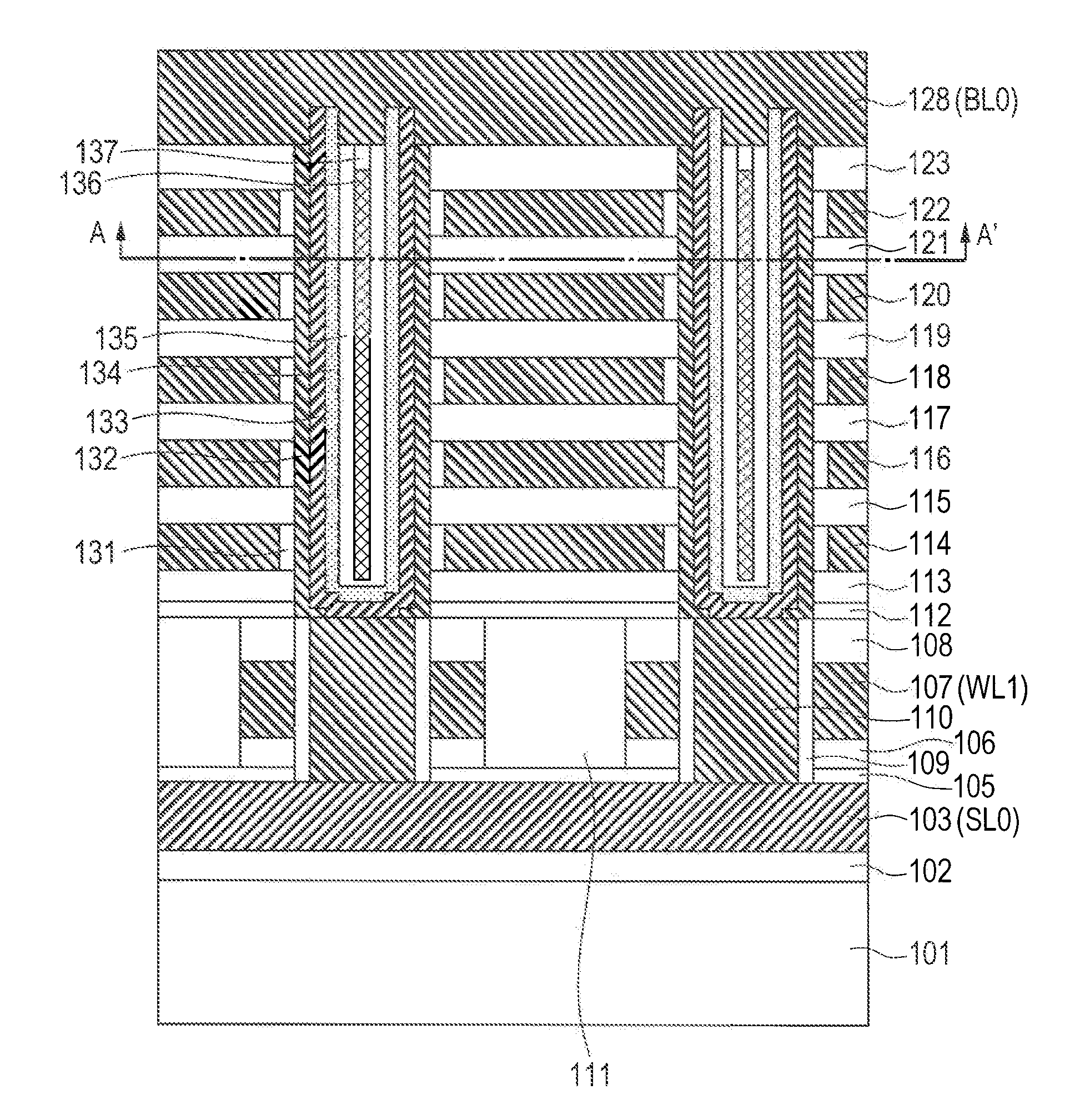
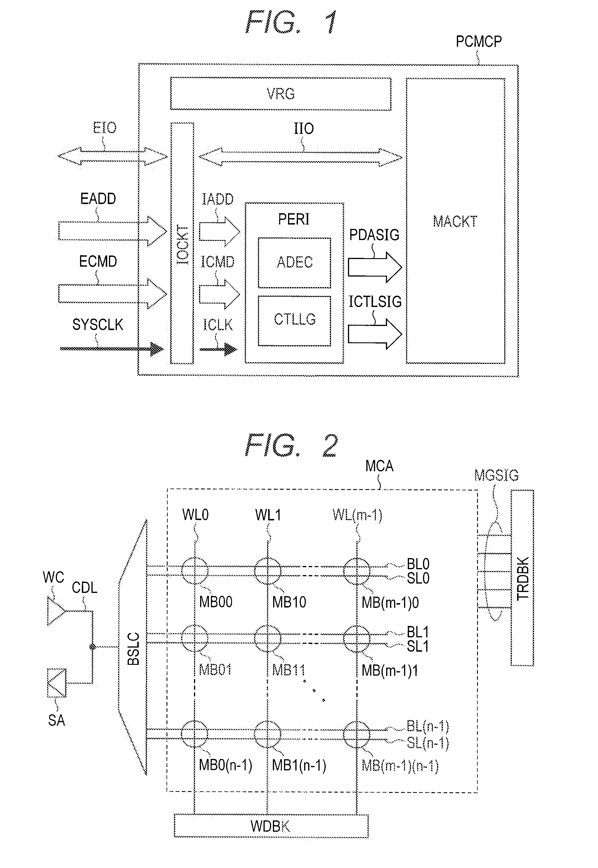
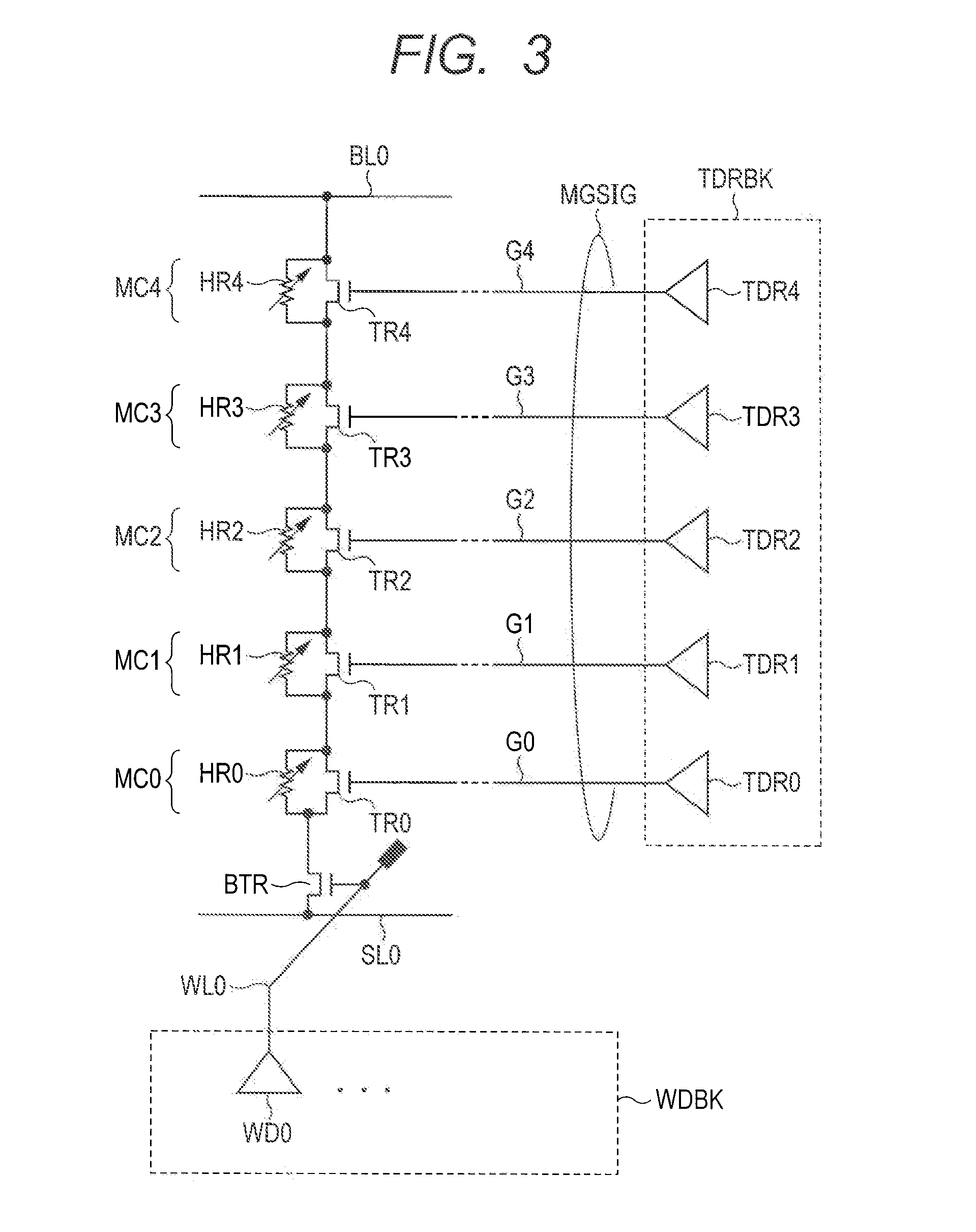
[0087]As described above, the semiconductor storage device according to the first embodiment comprises a set-dedicated memory cell MC0 in a memory block MB. By utilizing Joule heat generated by applying the set pulse current SETPLS to the memory cell MC0, same information is written concurrently into memory cells MC1 to MC4 in a same memory block MB, and then the reset operation is performed with respect to memory cells out of memory cells MC1 to MC4 in which the information should not be stored. Since reset operation time is shorter than set operation time, diffusion to peripheral memory cells of Joule heat generated by applying the reset pulse current is suppressed, whereby the information [0] can be written selectively.

[0088]That is, the semiconductor storage device according to the first embodiment is capable of preventing erroneous writing even when intervals among memory cells are reduced to an extent that Joule heat generated by applying the set pulse current SETPLS to the me...

second embodiment

[0107]As described above, the semiconductor storage device according to the second embodiment does not include a set-dedicated memory cell and writes information concurrently to all memory cells in a memory block by performing the set operation using any one of memory cells MC1 to MC4. Thereafter, the reset pulse current RSTPLS is applied to a memory cell, out of memory cells MC1 to MC4, in which the bit [0] should be stored. In such a manner, same operations as the first embodiment can be achieved.

[0108]Further, the semiconductor storage device according to the second embodiment selects a memory cell for the set operation according to the number of times of erasing and the number of times of recording stored in the table EPCTBL. In such a manner, concentrated application of the set pulse current SETPLS to a specific memory cell can be prevented. That is, deterioration of electric properties of memory cells to which the set pulse current SETPLS is applied can be suppressed.

[0109]Fur...

third embodiment

[0172]As described above, the semiconductor storage device according to the third embodiment has narrowed intervals among memory cells in the interconnect hole due to a half reduction of the effective memory area compared with a memory cell according to the first embodiment. However, after a pair of cell chains is erased (here, the set operation) concurrently by using memory cells for information storage, sequential reset operations are performed with respect to memory cells for information storage, whereby information can be recorded by selectively applying the current to memory cells in the memory block MB10.

[0173]The polysilicon diode PD according to the third embodiment may be provided instead of the block select transistor BTR according to the first and second embodiments. By using the polysilicon diode PD, the effective area can be reduced than the block select transistor BTR.


PUM


Abstract

A semiconductor storage device crystallizes variable resistive element material layers arranged on side surfaces of multiple semiconductor layers in a stacked structure concurrently by applying a first current to any one of semiconductor layers in the stacked structure, and thereafter applies a second current to semiconductor layers other than a semiconductor layer to which the first current was applied.

Description

CLAIM OF PRIORITY[0001]The present application claims priority from Japanese patent application JP 2011-105113 filed on May 10, 2011, the content of which is hereby incorporated by reference into this application.FIELD OF THE INVENTION[0002]The present invention relates to a semiconductor storage device.BACKGROUND OF THE INVENTION[0003]In a semiconductor storage device including a phase-change memory, a storage element is formed by using a Ge—Sb—Te based chalcogenide material (or phase-change material) containing at least antimony (Sb) and tellurium (Te) as a material of a recording layer. An element for selecting a memory cell is configured by using a vertical MOS transistor. Japanese Unexamined Patent Application Publication No. 2008-160004 cited below discloses an array configuration in which phase-change memory cells using a chalcogenide material and a vertical MOS transistor are stacked. According to FIG. 3 in the patent document, four memory cells and a vertical transistor TR5...

Claims


Application Information

Patent Timeline
Patent Type & Authority Applications(United States)
IPC IPC(8): G11C11/00
CPCH01L45/06G11C13/0004G11C13/0061G11C13/0069G11C2213/18H01L27/2481G11C2213/75H01L45/124H01L45/144H01L27/2454G11C2213/71H10B63/34H10B63/84H10N70/231H10N70/8265H10N70/8828
Inventor HANZAWA, SATORUMINEMURA, HIROYUKI
Owner HITACHI LTD
Why Eureka
Try Eureka