

Optical device packaging structure and optical device module
a technology of optical devices and packaging structures, applied in the field of optical device packaging structures and optical device modules, can solve the problems of loss of finished product rate, achieve the effects of reducing production costs, greatly improving production efficiency, and greatly enhancing the position accuracy of filter plates
- Summary
- Abstract
- Description
- Claims
- Application Information
AI Technical Summary
Benefits of technology
Problems solved by technology
Method used
Image

Examples
Embodiment Construction
[0037]For further illustrating the invention, experiments detailing an optical device packaging structure and an optical device module are described below. It should be noted that the following examples are intended to describe and not to limit the invention.
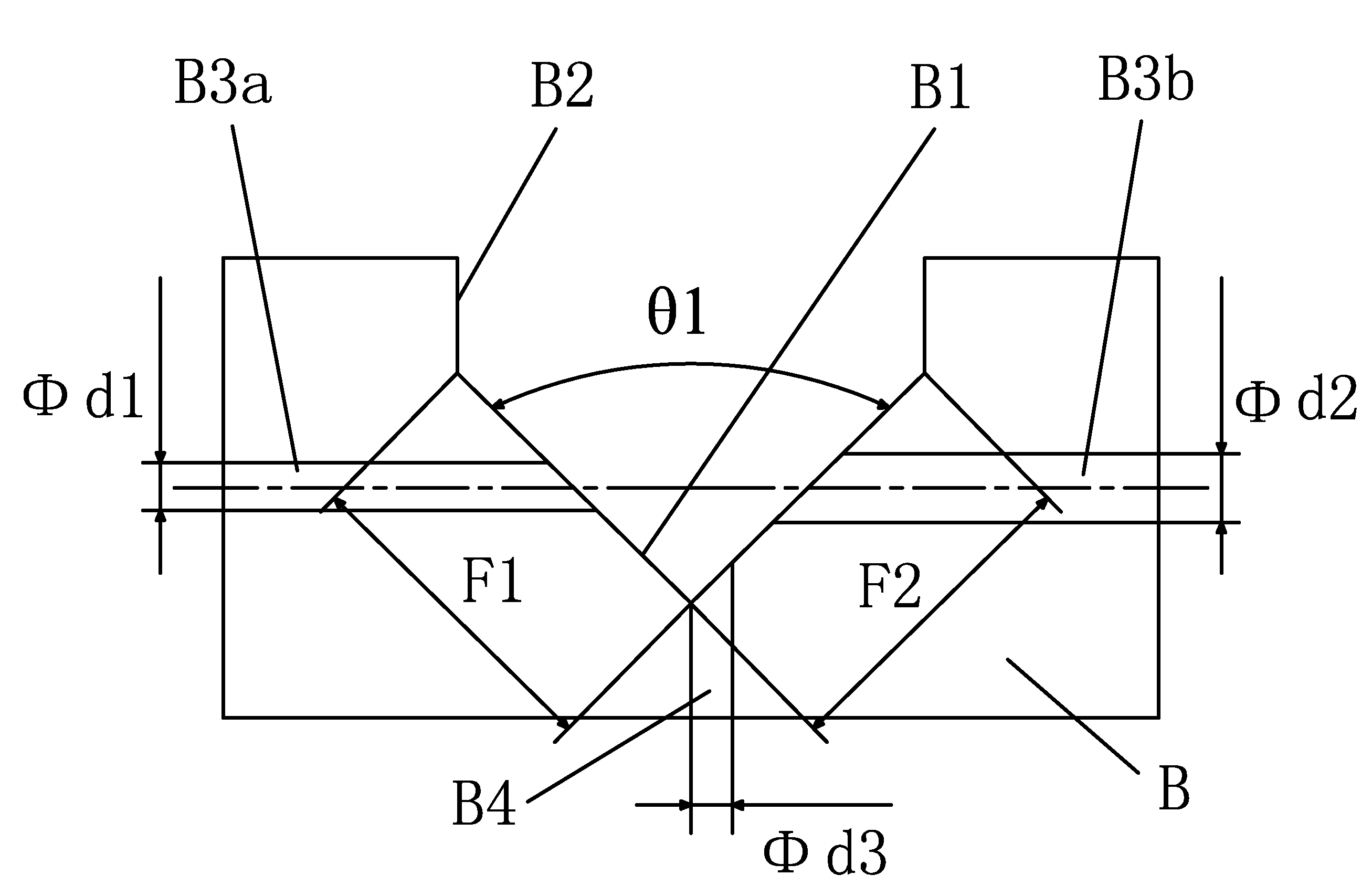
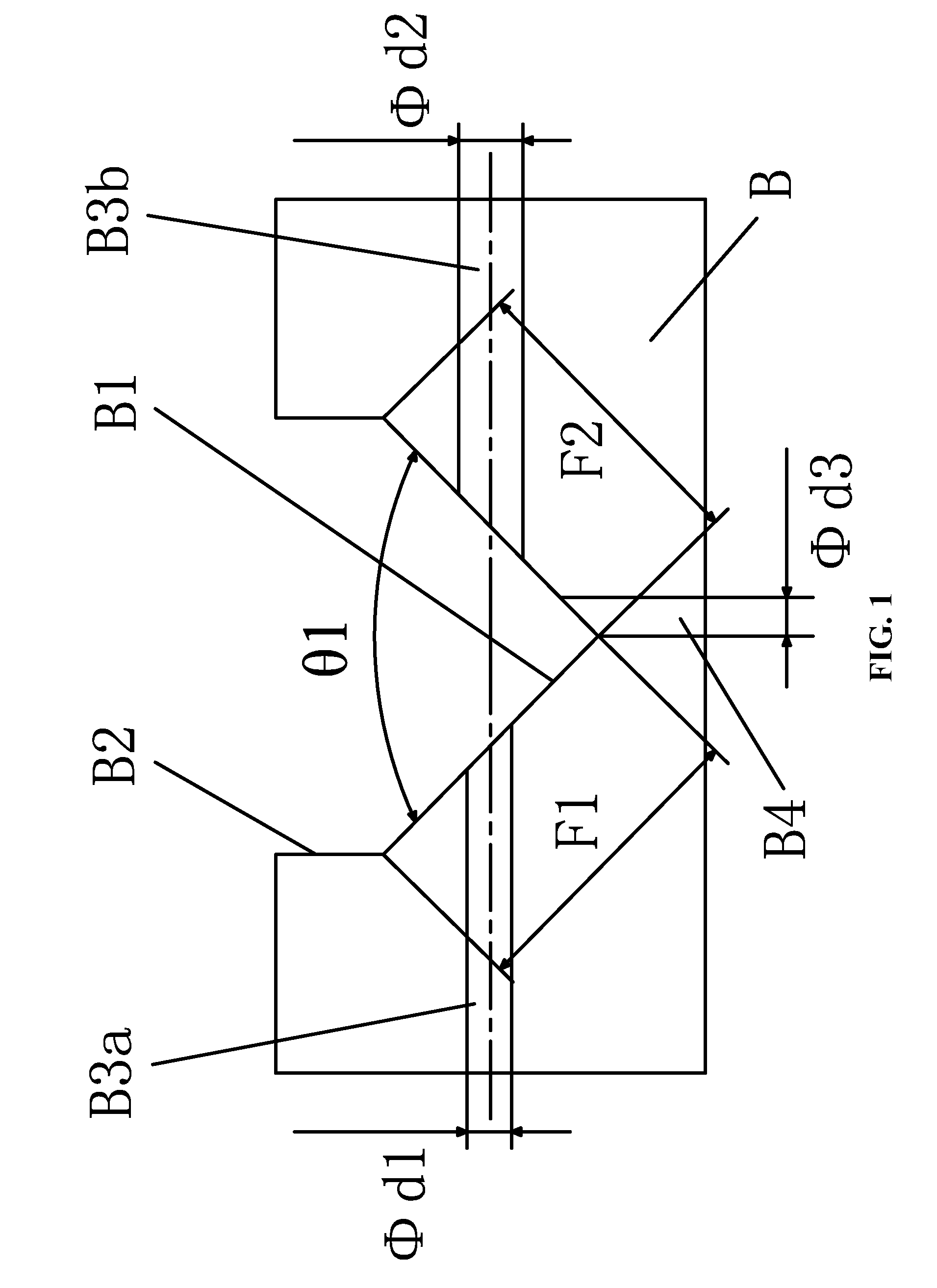
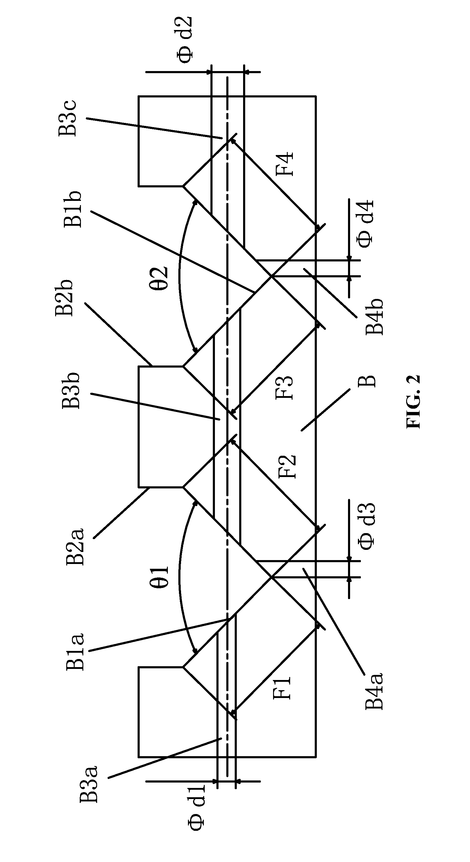
[0038]FIG. 1 is a basic structure diagram of an optical device packaging structure used for optical signal management.
[0039]An optical device packaging structure used for optical signal management comprises a main body B. One or more V-shaped grooves B1 are formed in the main body B, an optical signal transmission hole system communicated with two side walls of the V-shaped groove B1 is also arranged in the main body B and comprises optical signal transmission holes which are perpendicular and or parallel to the central line of the included angle of the V-shaped groove, and the included angle θ1 of the V-shaped groove is 90°±10°. The optimum included angle θ1 of the V-shaped groove is 90°.
[0040]A horizontal transmission hole per...
PUM
 Abstract
Description
Claims
Application Information