Semiconductor Processing System Having Multiple Decoupled Plasma Sources

a processing system and plasma source technology, applied in the direction of electrical equipment, basic electric elements, electric discharge tubes, etc., can solve the problems of inability to achieve the most desirable condition for dry etching, the type of independent ion concentration versus radical concentration cannot be achieved using the common plasma source typically used for thin film processing,

Inactive Publication Date: 2012-11-15
LAM RES CORP
View PDF3 Cites 384 Cited by
  • Summary
  • Abstract
  • Description
  • Claims
  • Application Information

AI Technical Summary

Problems solved by technology

Plasma sources utilized for thin film processing in semiconductor device fabrication are often unable to achieve the most desirable condition for dry etching due to the inability to separately control ion and rad

Method used


Image

  • Semiconductor Processing System Having Multiple Decoupled Plasma Sources
  • Semiconductor Processing System Having Multiple Decoupled Plasma Sources
  • Semiconductor Processing System Having Multiple Decoupled Plasma Sources

Examples


Embodiment Construction

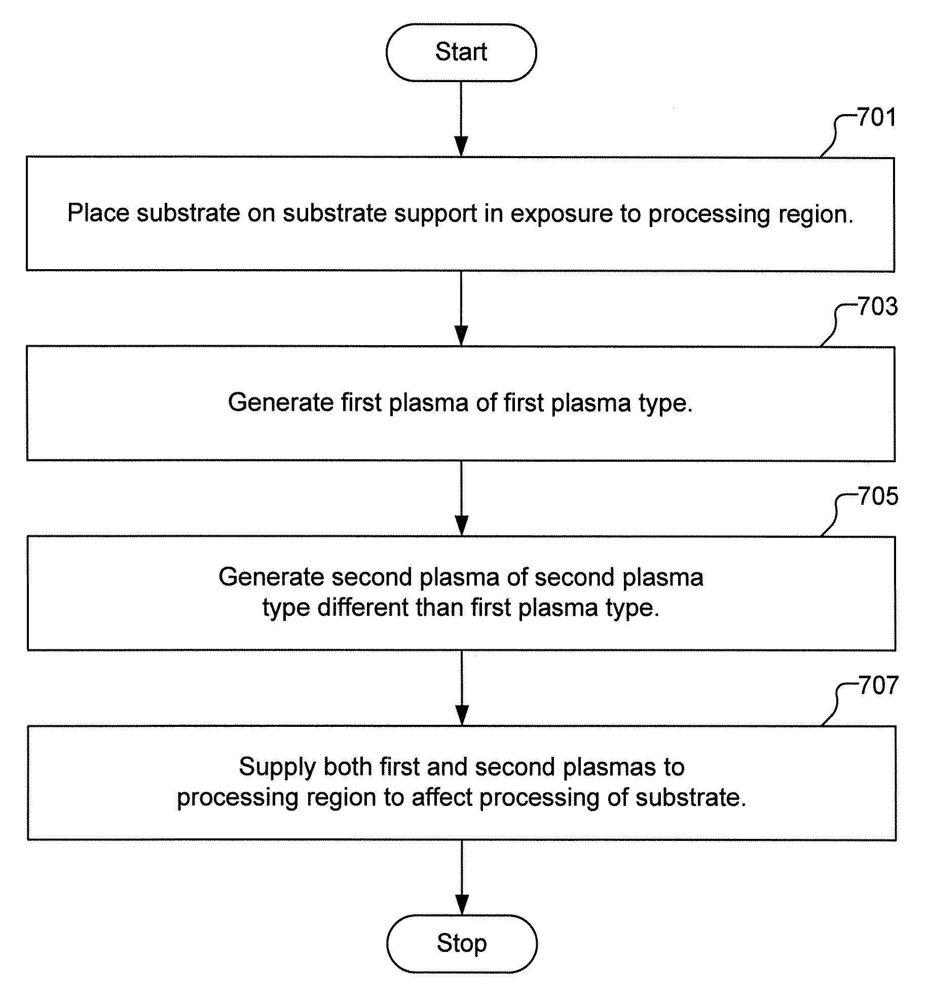
[0033]In the following description, numerous specific details are set forth in order to provide a thorough understanding of the present invention. It will be apparent, however, to one skilled in the art that the present invention may be practiced without some or all of these specific details. In other instances, well known process operations have not been described in detail in order not to unnecessarily obscure the present invention.

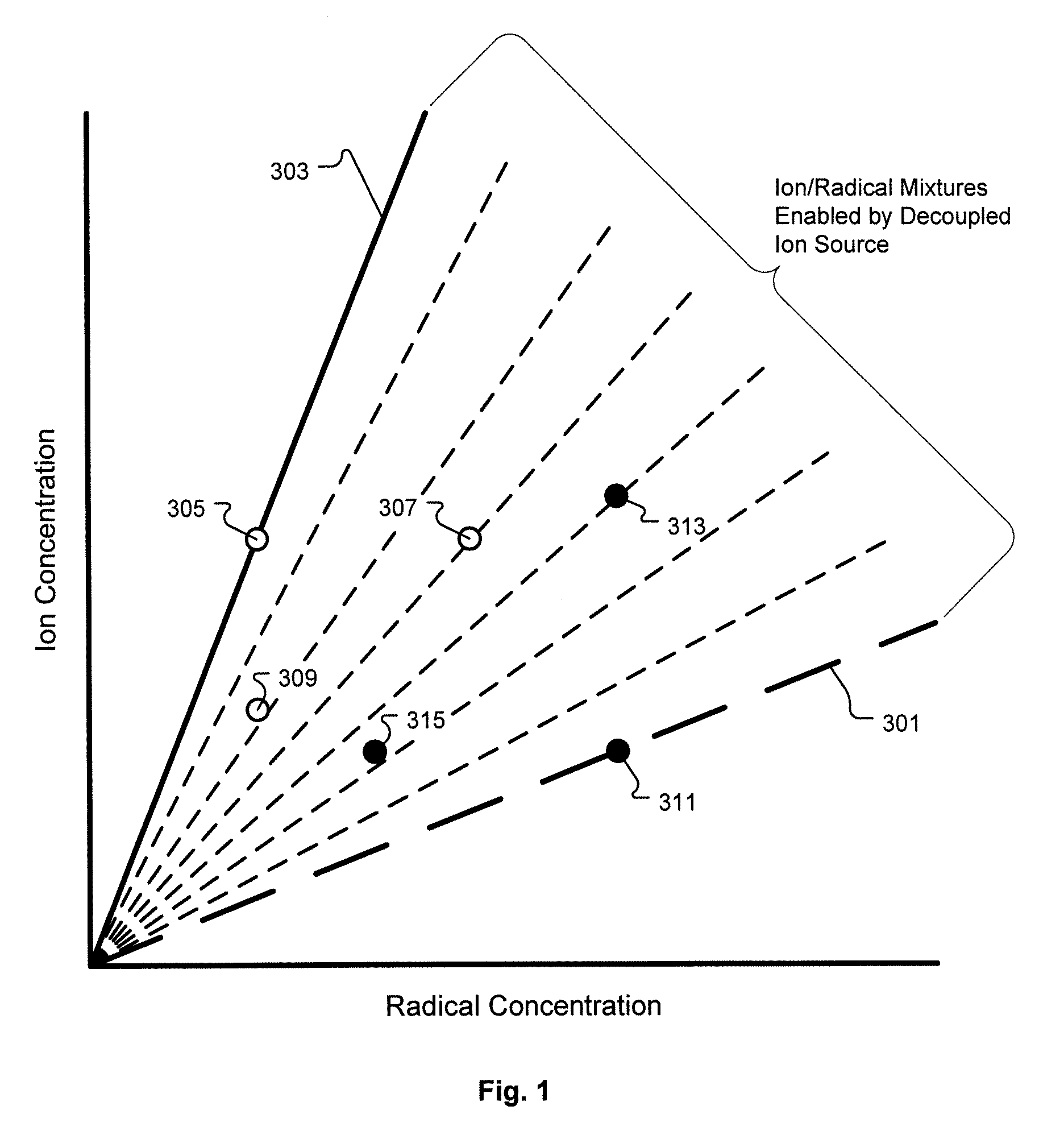
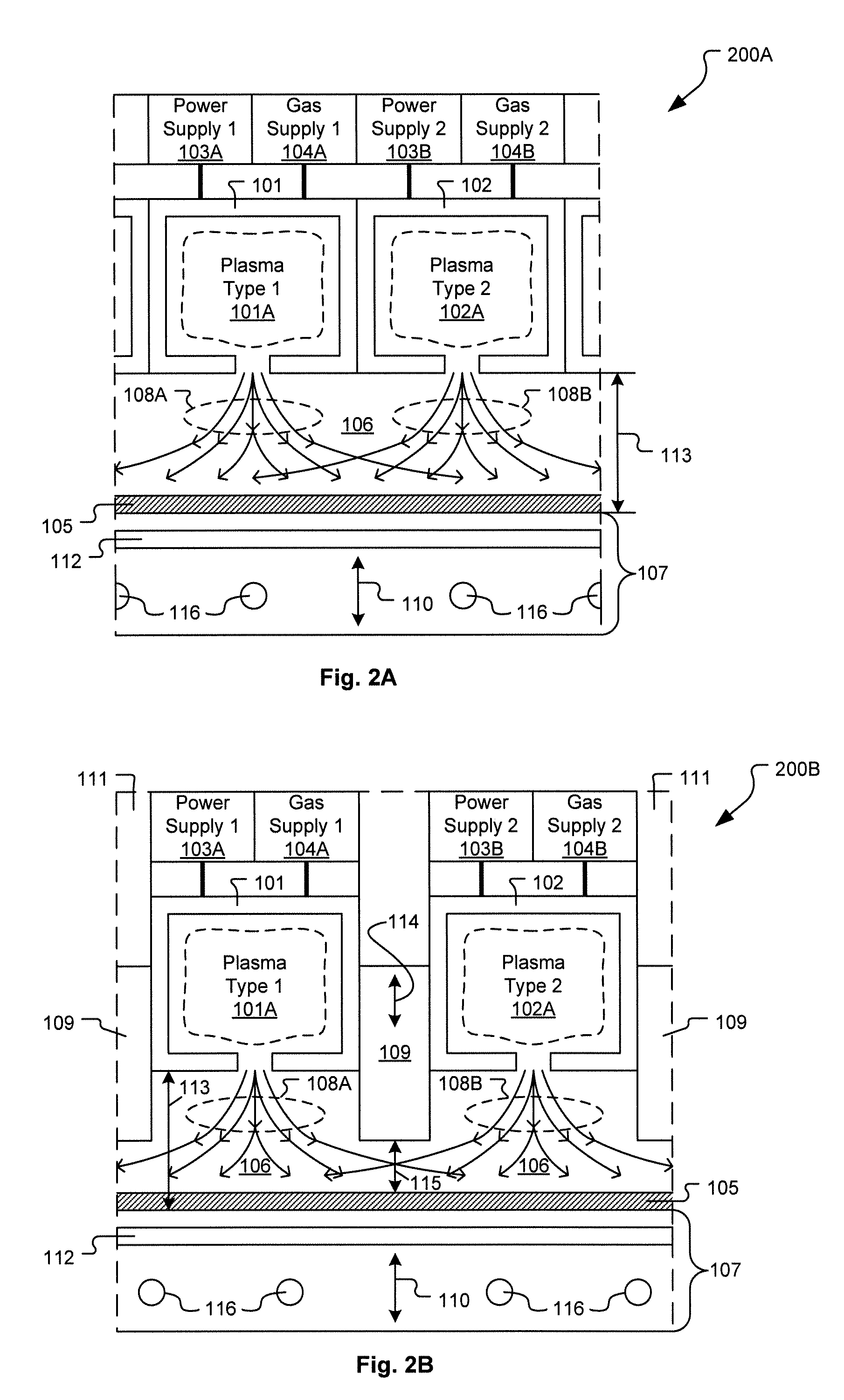
[0034]Various embodiments of the present invention include two or more types of plasma generating devices, such as plasma chambers, that can be independently operated using separate control parameters in order to achieve decoupled control of ion and radical concentrations within a plasma processing region to which the two or more types of plasma generating devices are fluidly connected, with a substrate to be processed disposed within the plasma processing region. For example, in one embodiment, a first plasma chamber can be operated to generate a first...


PUM

PropertyMeasurementUnit
Timeaaaaaaaaaa
Poweraaaaaaaaaa
Densityaaaaaaaaaa

Abstract

A semiconductor substrate processing system includes a substrate support defined to support a substrate in exposure to a processing region. The system also includes a first plasma chamber defined to generate a first plasma and supply reactive constituents of the first plasma to the processing region. The system also includes a second plasma chamber defined to generate a second plasma and supply reactive constituents of the second plasma to the processing region. The first and second plasma chambers are defined to be independently controlled.

Description

CROSS-REFERENCE TO RELATED APPLICATIONS[0001]This application is related to U.S. patent application Ser. No. ______ (Attorney Docket No.: LAM2P705B), filed on an even date herewith, and entitled “Semiconductor Processing System Having Multiple Decoupled Plasma Sources,” which is incorporated herein by reference in its entirety.BACKGROUND OF THE INVENTION[0002]Plasma sources utilized for thin film processing in semiconductor device fabrication are often unable to achieve the most desirable condition for dry etching due to the inability to separately control ion and radical concentrations in the plasma. For example, in some applications, the desirable conditions for plasma etching would be achieved by increasing the ion concentration in the plasma while simultaneously maintaining the radical concentration at a constant level. However, this type of independent ion concentration versus radical concentration control cannot be achieved using the common plasma source typically used for thi...

Claims


Application Information

Patent Timeline
IPC IPC(8): H01L21/3065C23F1/08H01L21/302
CPCH01J37/32899H01J37/32633
Inventor HOLLAND, JOHN PATRICKVENTZEK, PETER L.G.SINGH, HARMEETGOTTSCHO, RICHARD
Owner LAM RES CORP
Why Eureka
Try Eureka