Method and system of evaluating distribution of lattice strain on crystal material

Inactive Publication Date: 2012-11-22
LONGITUDE SEMICON S A R L
View PDF5 Cites 11 Cited by
  • Summary
  • Abstract
  • Description
  • Claims
  • Application Information

AI Technical Summary

Benefits of technology

[0018]The disclosure of the above Patent Documents and Non-patent Documents are incorporated herein in their entirety by reference thereto. The following analysis is given by the present invention. Since the above CBED and NBD methods are used for evaluation on one-dimensional points, it is insufficient to discuss the influence caused by lattice strain on device characteristics. Even with such evaluation method based on the CBED and NBD methods, in principle

Problems solved by technology

When an LSI device is manufactured, stress generated by use of various types of material causes lattice strain on a crystal structure used in a semiconductor device.
The lattice strain is a cause of a crystal defect or the like, resulting in device failure.
However, if the lattice strain is not controlled properly, a crystal defect leading to device malfunction is caused.
However, recent reduction in device size is making these conventional stress and lattice strain evaluation methods insufficient in spatial resolution, and it is becoming more difficult to obtain sufficient results.
Since the above CBED and NBD met

Method used


Image

  • Method and system of evaluating distribution of lattice strain on crystal material
  • Method and system of evaluating distribution of lattice strain on crystal material
  • Method and system of evaluating distribution of lattice strain on crystal material

Examples


first exemplary embodiment

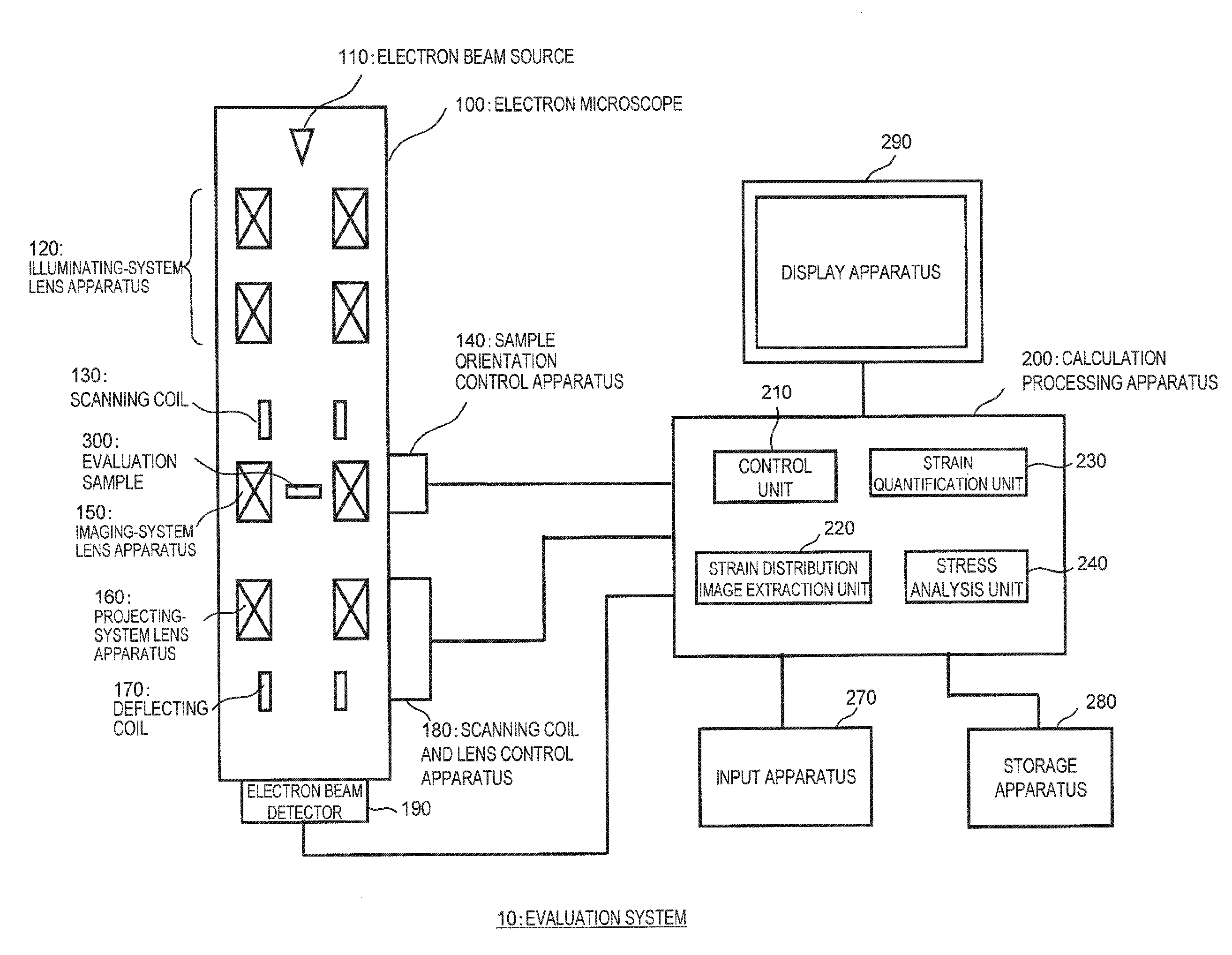
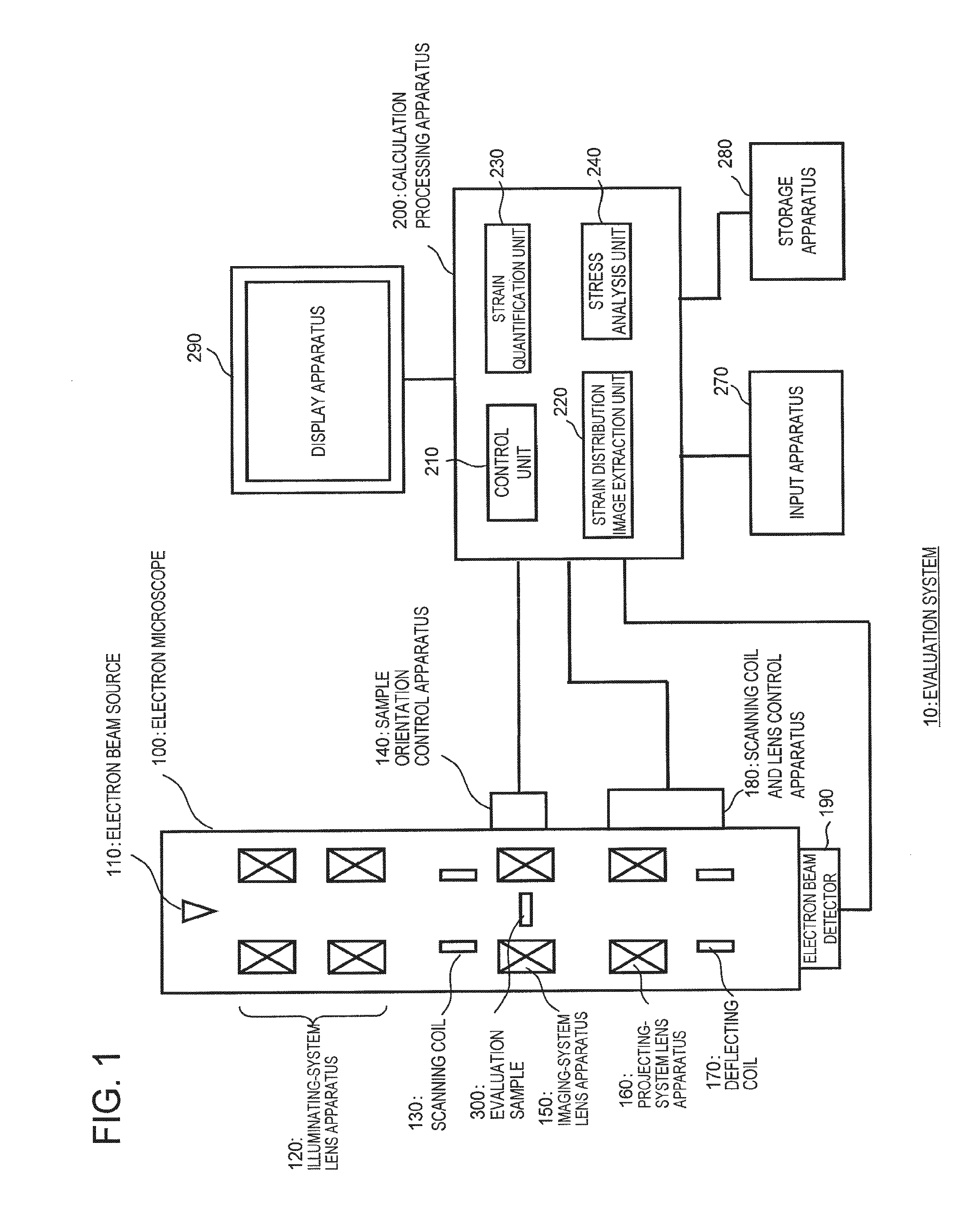
[0044]FIG. 1 is a block diagram illustrating an overall configuration of a system 10 of evaluating a distribution of lattice strain on crystal material according to a first exemplary embodiment. The evaluation system 10 in FIG. 1 includes: a scanning transmission electron microscope 100; and a calculation processing apparatus 200 controlling the electron microscope 100 and processing measurement data obtained by the electron microscope 100.

[0045]The electron microscope 100 includes an electron beam source 110 outputting an electron beam used for observing an evaluation sample 300; an illuminating-system lens apparatus 120 using the electron beam outputted from the electron beam source 110 to illuminate the evaluation sample 300; and an imaging-system lens apparatus 150 functioning as an objective lens focusing an electron beam on a minute spot region of the evaluation sample 300. An electron beam transmitted by the evaluation sample 300 or an electron beam diffracted in the forward ...

second exemplary embodiment

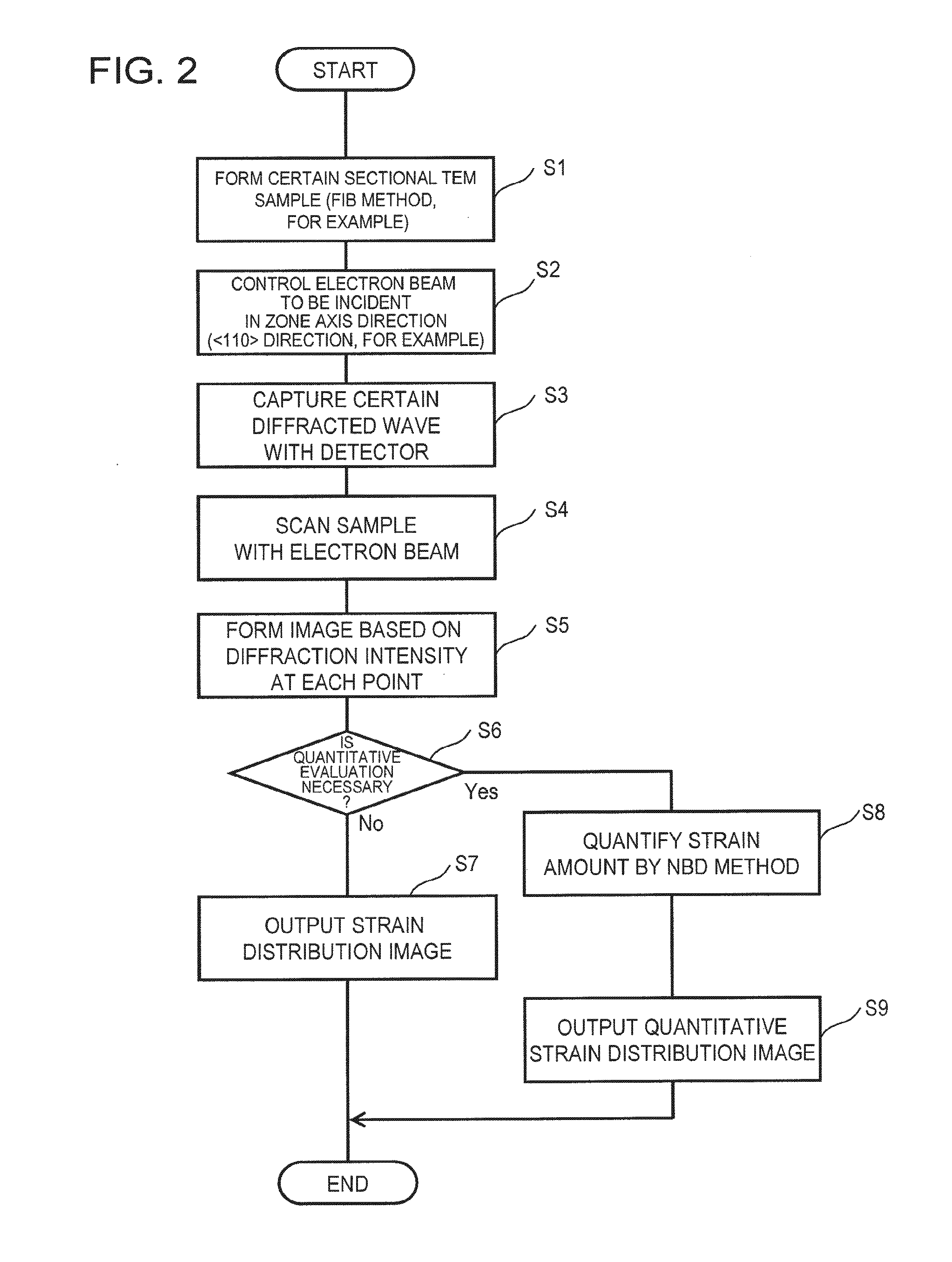
[0062]In the first exemplary embodiment, outputting a quantitative strain distribution image in each direction is described. In a second exemplary embodiment, based on the output results according to the first exemplary embodiment, a principal strain distribution and a shear strain distribution in an arbitrary direction are outputted to grasp the cause of crystal strain and to predict the possibility of occurrence of a crystal defect. FIG. 7 is a flow chart illustrating a process procedure according to the second exemplary embodiment.

[0063]Before the second exemplary embodiment is described, evaluation examples of lattice strain caused when a shallow trench isolation (STI) generally used in a silicon LSI device causes stress to an active region will be described with reference to FIGS. 8A to 8D. FIG. 8A is a plan view when an STI interface is formed in alignment with the crystal orientation in an active region. FIG. 8B is an enlarged view of a portion near the interface. FIG. 8C is ...

third exemplary embodiment

[0074]The calculation processing apparatus 200 in the evaluation system 10 in FIG. 1 is not necessarily a dedicated calculation processing apparatus. By causing a general-purpose computer such as an EWS or a PC to execute a dedicated evaluation program stored in the storage apparatus 280, the general-purpose computer, the electron microscope 100, and peripheral apparatuses such as the sample orientation control apparatus 140, the scanning coil and lens control apparatus 180, and the electron beam detector 190 can be allowed to function as the evaluation system 10. In this case, peripheral apparatuses connectable to the general-purpose computer can be used as the display apparatus 290, the input apparatus 270, and the storage apparatus 280. In addition, by causing the general-purpose computer to execute the evaluation program stored in the storage apparatus 280, the general-purpose computer can be allowed to function as the calculation processing apparatus 200 including the control u...


PUM


Abstract

A crystal material lattice strain evaluation method includes illuminating a sample having a crystal structure with an electron beam in a zone axis direction, and selectively detecting a certain diffracted wave diffracted in a certain direction among a plurality of diffracted waves diffracted by the sample. The method further includes repeating the illuminating step and the selectively detecting step while scanning the sample, and obtaining a strain distribution image in a direction corresponding to the certain diffracted wave from diffraction intensity at each point of the sample.

Description

TECHNICAL FIELDREFERENCE TO RELATED APPLICATION[0001]This application is based upon and claims the benefit of the priorities of Japanese patent application No. 2011-112618, filed on May 19, 2011 and Japanese patent application No. 2012-034676, filed on Feb. 21, 2012 the disclosure of which is incorporated herein in its entirety by reference thereto.[0002]The present invention relates to a method and a system of evaluating a distribution of lattice strain on crystal material. In particular, it relates to a method and a system of evaluating a distribution of lattice strain on crystal material used in a semiconductor device or the like by using electron beam diffraction.BACKGROUNDDESCRIPTION OF THE RELATED ART[0003]When an LSI device is manufactured, stress generated by use of various types of material causes lattice strain on a crystal structure used in a semiconductor device. Such lattice strain is one of the important physical quantities that exhibit crystal material properties. The...

Claims


Application Information

Patent Timeline
IPC IPC(8): H01J37/26
CPCG01N23/2055G01N23/20058H01J2237/2802H01J37/2955
Inventor NOJIMA, KAZUHIRO
Owner LONGITUDE SEMICON S A R L
Why Eureka
Try Eureka