Semiconductor Device

a technology of semiconductors and circuits, applied in the direction of power consumption reduction, pulse techniques, instruments, etc., can solve the problems of high leakage current, more severe problems in dynamic logic circuits than in static logic circuits,

Inactive Publication Date: 2012-11-22
SEMICON ENERGY LAB CO LTD
View PDF4 Cites 36 Cited by
  • Summary
  • Abstract
  • Description
  • Claims
  • Application Information

AI Technical Summary

Benefits of technology

[0016]It is possible to provide a logic circuit including such a transistor whose off-state current is low and thus having a property of being d

Problems solved by technology

Thus, leakage current from transistors causes more severe problems in dynamic logic circuits than in static logic circuits.
For example, in a dynamic ci

Method used


Image

  • Semiconductor Device
  • Semiconductor Device
  • Semiconductor Device

Examples


embodiment 1

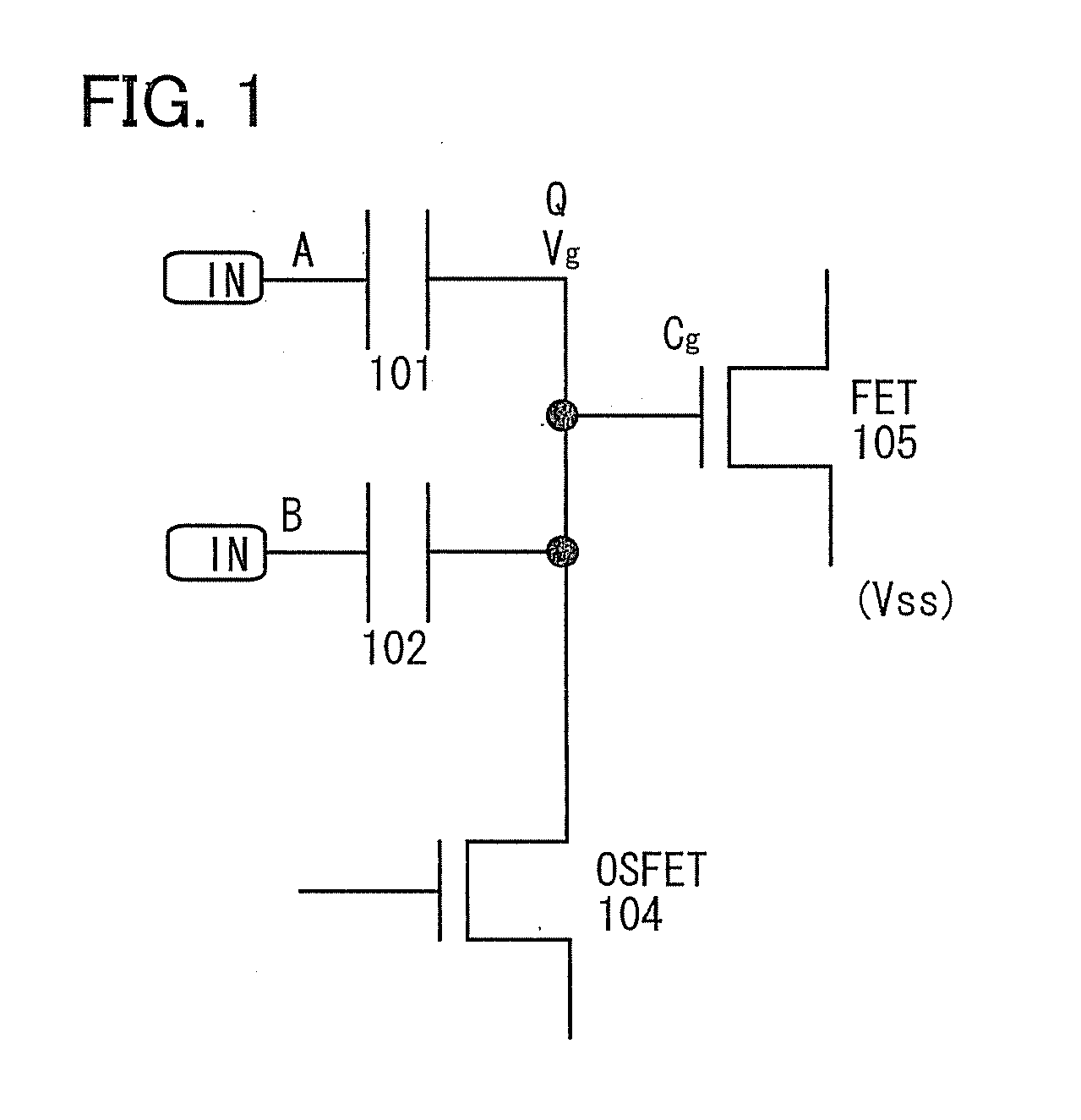
[0047]In this embodiment, a basic structure of a logic circuit will be described. FIG. 1 illustrates a logic circuit including a first capacitor 101, a second capacitor 102, a first transistor (OSFET) 104 whose off-state current is low, and a second transistor (FET) 105.

[0048]The first transistor is also referred to as an OSFET because it includes an oxide semiconductor in a channel formation region. A channel formation region including an oxide semiconductor has n-type conductivity in many cases; thus, the first transistor is an n-channel transistor. The off-state current of such a transistor including an oxide semiconductor in a channel formation region is low. The details of the transistor will be described in the following embodiment.

[0049]A transistor including silicon in a channel formation region is used as the second transistor since the off state-current of the second transistor is not necessarily as low as that of the first transistor. Such a transistor is referred to as a...

embodiment 2

[0089]In this embodiment, a basic structure of a logic circuit in which the second transistor described in Embodiment 1 is a p-channel transistor will be described. FIG. 3 illustrates a logic circuit including the first capacitor 101, the second capacitor 102, the first transistor (OSFET) 104 whose off-state current is low, and a second transistor (FET) 205. The second transistor is a p-channel transistor.

[0090]The first capacitor 101, the second capacitor 102, the first transistor 104, and the second transistor 205 are electrically connected to one another as illustrated in FIG. 3. One electrode of the first capacitor 101 is electrically connected to a gate of the second transistor 205. One electrode of the second capacitor 102 is electrically connected to the gate of the second transistor 205. The one electrode of the second capacitor 102 is also electrically connected to one of a source and a drain of the first transistor 104. Since the first transistor 104 is an n-channel transi...

embodiment 3

[0128]In this embodiment, a logic circuit in which the circuit described in Embodiment 1 is combined with the circuit described in Embodiment 2 will be described.

[0129]In the circuit described in Embodiment 1 (see FIG. 1), the second transistor 105 is an n-channel transistor. In the circuit described in Embodiment 2 (see FIG. 3), the second transistor 205 is a p-channel transistor. These circuits can be combined to form a CMOS circuit.

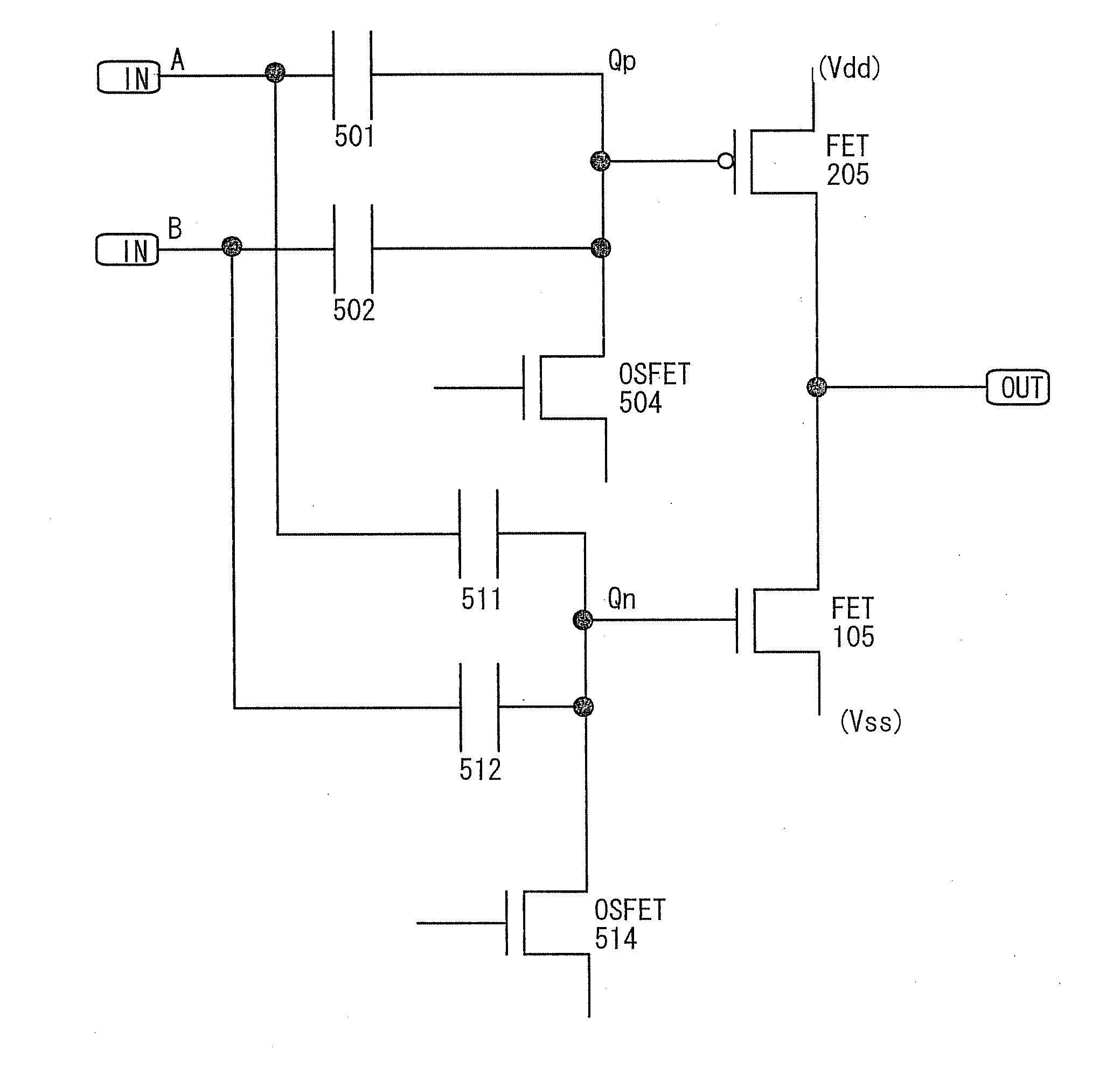
[0130]FIG. 25 illustrates a CMOS circuit including a first capacitor 501, a second capacitor 502, a third capacitor 511, a fourth capacitor 512, a first transistor (OSFET) 504, a second transistor (OSFET) 514, a third transistor 205, and a fourth transistor 105. The third transistor 205 and the fourth transistor 105 are a p-channel transistor and an n-channel transistor, respectively.

[0131]These components are electrically connected to one another as illustrated in FIG. 25. One electrode of the first capacitor 501 is electrically connected to the termi...


PUM


Abstract

As semiconductor devices including semiconductors, logic circuits are given. Logic circuits include dynamic logic circuits and static logic circuits and are formed using transistors and the like. Dynamic logic circuits can store data for a certain period of time. Thus, leakage current from transistors causes more severe problems in dynamic logic circuits than in static logic circuits. A logic circuit includes a first transistor whose off-state current is small and a second transistor whose gate is electrically connected to the first transistor. Electric charge is supplied to a node of the gate of the second transistor through the first transistor. Electric charge is supplied to the node through a first capacitor and a second capacitor. On/off of the second transistor is controlled depending on a state of the electric charge. The first transistor includes an oxide semiconductor in a channel formation region.

Description

BACKGROUND OF THE INVENTION[0001]1. Field of the Invention[0002]The present invention relates to a semiconductor device including a semiconductor.[0003]2. Description of the Related Art[0004]As semiconductor devices including semiconductors, logic circuits are given. Logic circuits include dynamic logic circuits and static logic circuits and are formed using transistors and the like. Dynamic logic circuits can store data for a certain period of time. Thus, leakage current from transistors causes more severe problems in dynamic logic circuits than in static logic circuits. Leakage current is attributed to off-state current flowing when transistors are turned off.[0005]For example, in a dynamic circuit, leakage current is high when a MOS transistor which controls supply of electric charge to a dynamic node is off, which is regarded as a problem. To solve this problem, a structure has been suggested in which a MOS transistor circuit is inserted into a current path to a dynamic node (Pa...

Claims


Application Information

Patent Timeline
IPC IPC(8): G11C5/14H03K19/173H01L27/06
CPCH03K19/0013H01L27/1225H01L27/12H03K19/0944G11C7/10H01L27/1214H01L27/1255
Inventor KATO, KIYOSHI
Owner SEMICON ENERGY LAB CO LTD
Why Eureka
Try Eureka