Method and device for obtaining a multicrystalline semiconductor material, in particular silicon

a multi-crystalline semiconductor and semiconductor material technology, applied in the direction of saccharide production, crystal growth process, food science, etc., can solve the problems of increasing the increasing the cost and overall dimensions of the furnace, and requiring long steps of melting solid semiconductor materials to be refined, so as to reduce the overall dimensions and the level of energy consumption of the necessary equipment, and the effect of simple and inexpensive implementation

Inactive Publication Date: 2012-11-29
SAET
View PDF5 Cites 17 Cited by
  • Summary
  • Abstract
  • Description
  • Claims
  • Application Information

AI Technical Summary

Benefits of technology

[0006]The aim of the present invention is to overcome the drawbacks of the known art by providing a device and a method for obtaining a multicrystalline semiconductor material, typically silicon, with a “solar” degree of purity that will be simple and inexpensive to implement, will enable a reliable and effective control of the thermal flows, and will enable reduction of the overall dimensions and the levels of energy consumption of the necessary equipment.

Problems solved by technology

In known DSS furnaces, whether they be provided with heating with electrical resistors or with induction heating, this is obtained by using heavy insulating layers, which increase the costs and the overall dimensions of the furnace and, consequently, the levels of energy consumption for managing it.
Furthermore, the step of melting of the solid semiconductor material to be refined requires long times and high levels of energy consumption.

Method used


Image

  • Method and device for obtaining a multicrystalline semiconductor material, in particular silicon
  • Method and device for obtaining a multicrystalline semiconductor material, in particular silicon
  • Method and device for obtaining a multicrystalline semiconductor material, in particular silicon

Examples


Embodiment Construction

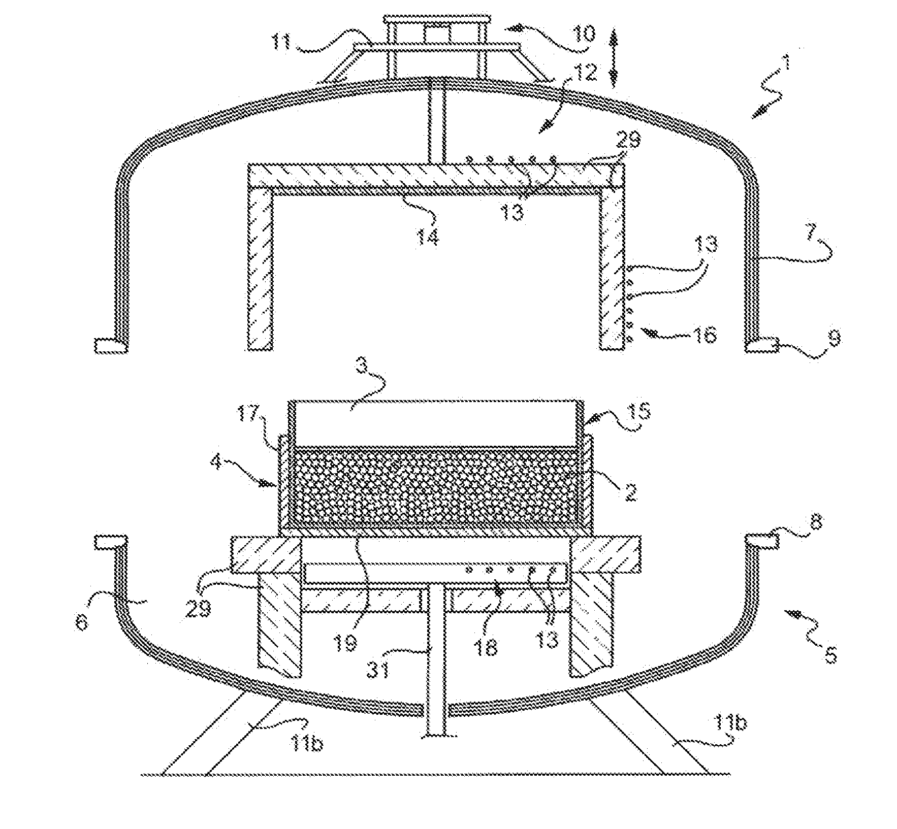
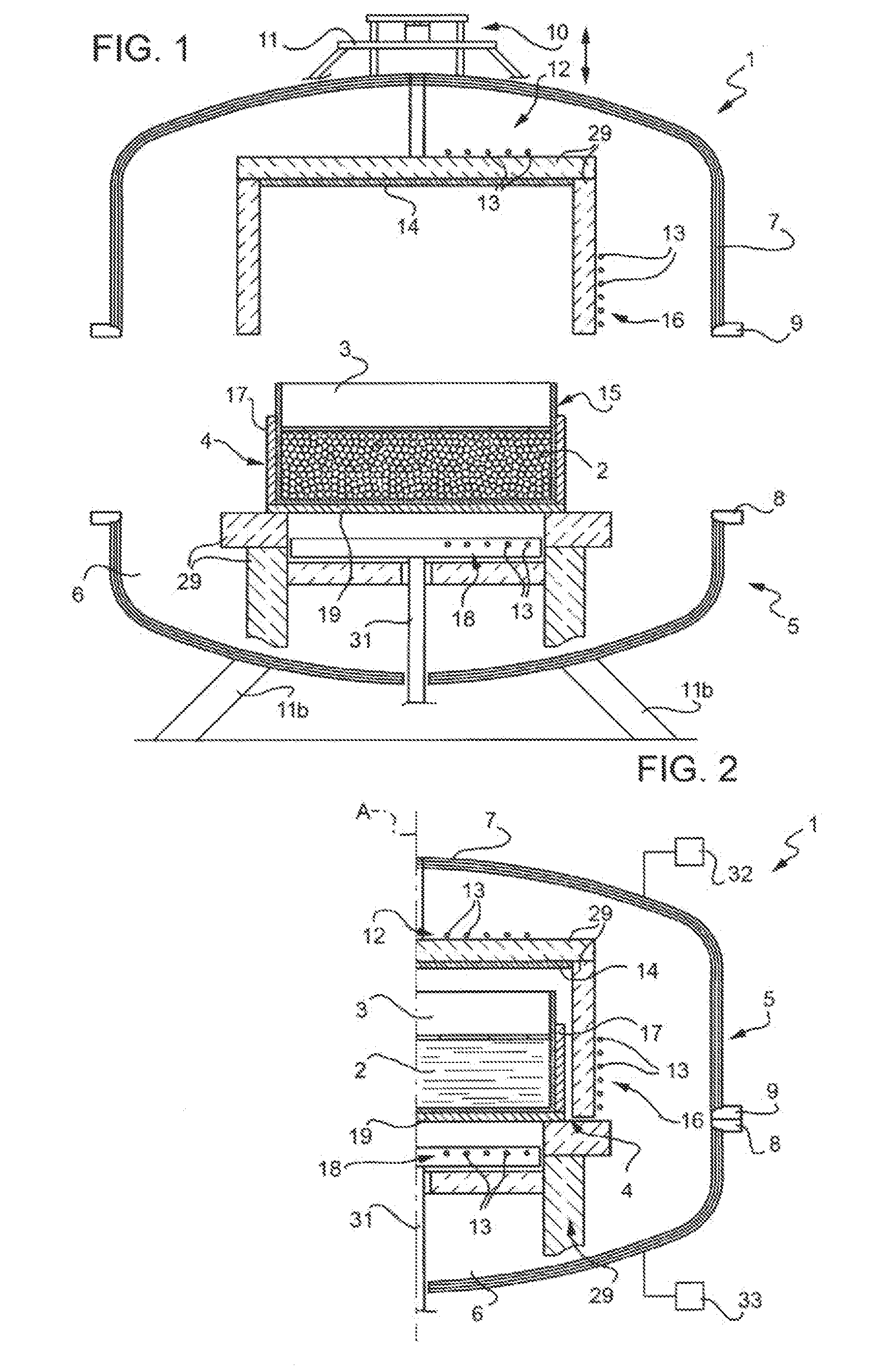
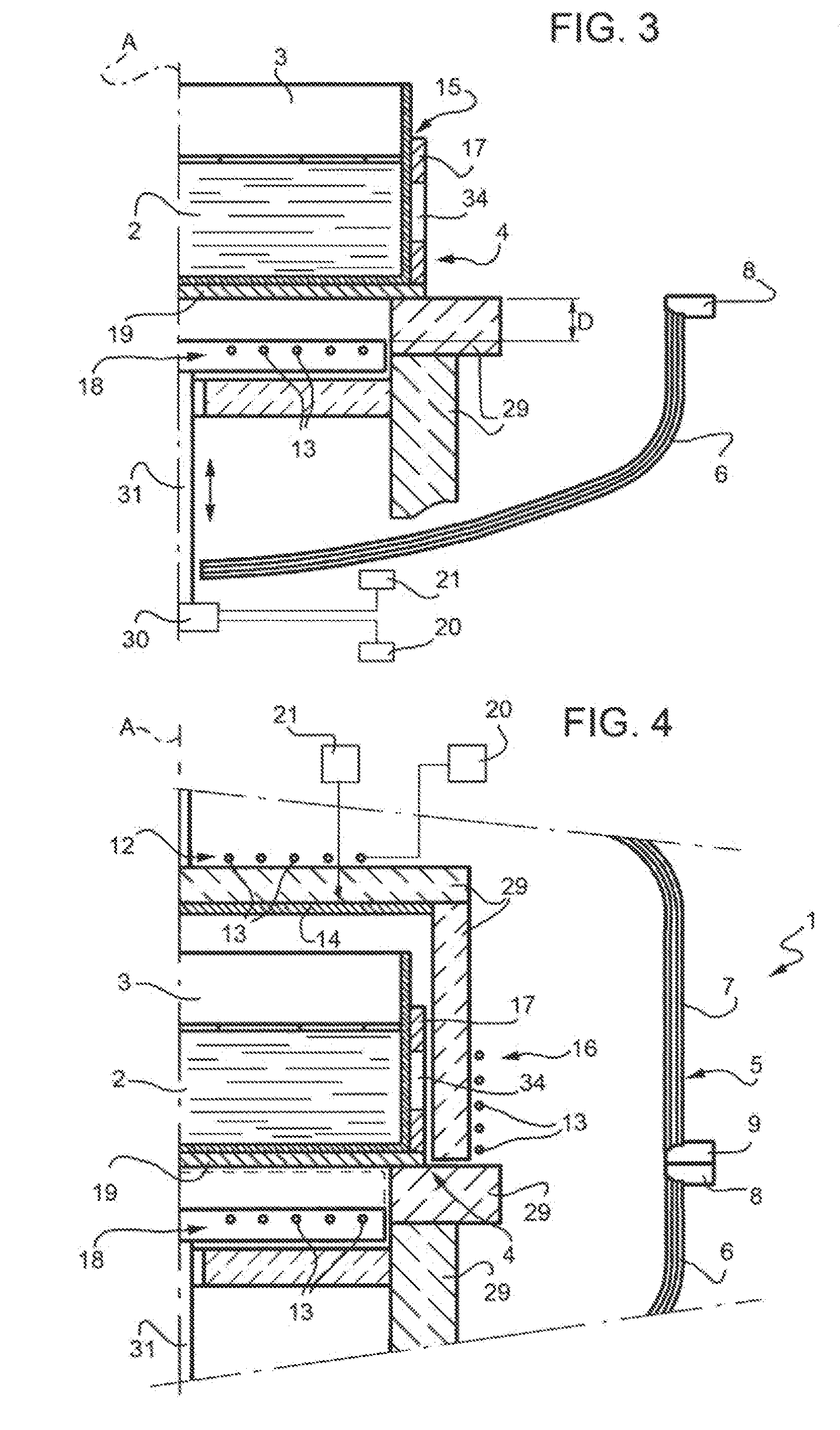
[0026]With reference to FIGS. 1 to 4, designated as a whole by 1 is a device for melting and subsequent directional solidification of a semiconductor material 2, typically to obtain multicrystalline silicon with solar degree of purity.

[0027]The device 1 comprises: at least one crucible 3 for the semiconductor material 2, preferably made of quartz or ceramic material, removably housed in a cup-shaped graphite container 4; and a fluid-tight casing 5, housing inside it the graphite container 4 and delimited by a bottom half-shell 6 and by a top half-shell 7, which are cup-shaped; the latter, which are preferably made of steel, are normally coupled on top of one another (FIG. 2) with their concavities facing one another and respective edges 8, 9 provided with appropriate gaskets (not illustrated) butted together in a fluid-tight way.

[0028]The device 1 further comprises means 10 for moving vertically the top half-shell 7 away from the bottom half-shell 6, in the case in point in such a w...


PUM

PropertyMeasurementUnit
conduction temperatureaaaaaaaaaa
temperatureaaaaaaaaaa
frequencyaaaaaaaaaa

Abstract

A device for obtaining multicrystalline silicon, including: at least one crucible, removably housed in a cup-shaped graphite container; a fluid-tight casing, including a fixed bottom half-shell and a vertically mobile top half-shell; a top induction coil, set facing, with interposition of a graphite plate, the crucible, a lateral induction coil and a bottom induction coil vertically mobile for varying the distance from the bottom wall; and means for a.c. electrical supply of the induction coils separately from one another; at least the lateral induction coil includes a plurality of plane turns set on top of one another, and means for selectively short-circuiting, supplying or not supplying the turns, all together or separately one or more at a time and for varying the frequency of supply thereof all together or separately one or more at a time.

Description

TECHNICAL FIELD[0001]The present invention relates to a method and to a device for obtaining a multicrystalline semiconductor material, in particular silicon, by melting of the semiconductor material and subsequent directional solidification thereof.BACKGROUND ART[0002]The demand for semiconductor material, in particular silicon, with a high degree of purity, referred to as “solar purity”, is increasingly higher, in so far as said material is necessary for the production of high-efficiency photovoltaic cells.[0003]To obtain such a material refinements are first made by means of traditional metallurgical method, and, finally, an ingot is formed, from which the wafers necessary for production of the photovoltaic cells can then be sectioned. Said ingot is formed with a method known as “directional solidification system” (DSS), i.e., by melting the semiconductor material in a crucible and then causing a directional solidification thereof to obtain at the end multicrystalline silicon.[00...

Claims


Application Information

Patent Timeline
Patent Type & Authority Applications(United States)
IPC IPC(8): B01D9/00H05B6/22
CPCB22D27/045C30B11/003C30B29/06C30B35/00H05B6/44H05B6/24H05B6/36H05B6/367F27B14/14B22D27/04C30B11/00
Inventor DUGHIERO, FABRIZIOFORZAN, MICHELECISCATO, DARIOCESANO, MARIOLINOCRIVELLO, FABRIZIOBERNABINI, PAOLO
Owner SAET
Why Eureka
Try Eureka