Unlock instant, AI-driven research and patent intelligence for your innovation.

Estimation of presence of void in through silicon via (TSV) based on ultrasound scanning

a silicon via and ultrasound scanning technology, applied in semiconductor/solid-state device testing/measurement, semiconductor/solid-state device details, instruments, etc., can solve the problems of void (gap), uneven thickness of plating material, and low rigidity of the board itsel

Inactive Publication Date: 2012-12-06
IBM CORP
View PDF3 Cites 7 Cited by
  • Summary
  • Abstract
  • Description
  • Claims
  • Application Information

AI Technical Summary

Benefits of technology

[0024]In a first aspect of the invention, a method for estimating a presence of a void in a through silicon via (TSV) on the basis of ultrasound scanning is provided. The method includes preparing a board in which a plurality of TSVs are arranged, selecting one or more TSVs belonging to a test element group (TEG) from among the plurality of TSVs, where physical obstruction in a vicinity of the TEG being less than the physical obstruction in a vicinity of other TSVs that do not belong to the TEG in scanning over a board surface, scanning at least one of the one or more TSVs belonging to the TEG over the board surface and estimating that a void is present in the other TSVs not belonging to the TEG on the basis of a result of the scanning.
[0025]In a second aspect of the invention, a board is provided. The board includes a plurality of through silicon vias (TSVs) which are arranged to estimate a presence of a void in the TSVs, where one or more TSVs belonging to a test element group (TEG) are selected from among the plurality of TSVs, and physical obstruction in a vicinity of the one or more TSVs being less than the physical obstruction in a vicinity of other TSVs not belonging to the TEG in scanning on a board surface.
[0026]In a third aspect of the invention, an apparatus for estimating a presence of a void in a through silicon via (TSV) on the basis of ultrasound scanning is provided. The apparatus includes a display, an imaging processing unit, a computation processing unit, a control circuit, an AD / DA conversion unit, a transmission unit, a receiving unit, a prepared board in which a plurality of TSVs are arranged, where one or more TSVs belonging to a test element group (TEG) from among the plurality of TSVs, and physical obstruction in a vicinity of the TEG being less than physical obstruction in a vicinity of other TSVs that do not belong to the TEG in scanning over a board surface.

Problems solved by technology

Thus the board is required to be supported by the support substrate because the rigidity of the board itself is low.
In contrast, for an unsuccessful example illustrated on the right side in the drawing, the plating material is not sufficiently spread and does not reach the aluminum layer, and a void (gap) occurs.
Such a defective mode impedes conduction between the etching stop layer and the metal of the TSV and makes the TSV inactive.
To make matters worse, because the opening of the board is covered, such a void is hidden, cannot be sought in a surface inspection, and remains as a defect.
If the seed layer is imperfect and a sufficient electric current is not transmitted to a deep area, this can cause a void.
However, a satisfactory method for detecting a void that remains hidden in small-diameter TSVs arranged at a narrow pitch has not been known yet.
An X-ray inspection known as an existing method requires a very long time for capturing an image.
Thus, inspecting the entire surface is impractical from a cost standpoint.
However, typically, because a bump electrode or a wiring layer is present directly above or below the void in the TSV and the wiring and the bump shape on the surface layer as “physical obstruction” scatters ultrasound, it is difficult to detect a void with a ultrasonic microscope using echoes of an ultrasonic wave.
However, the disclosed technique does not deal with estimating the presence of a void in a through silicon via (TSV) and, in addition, Japanese Patent Application Publication No. 2000-82121 has no discussion of a test element group (TEG) having less physical obstruction.

Method used


Image

  • Estimation of presence of void in through silicon via (TSV) based on ultrasound scanning
  • Estimation of presence of void in through silicon via (TSV) based on ultrasound scanning
  • Estimation of presence of void in through silicon via (TSV) based on ultrasound scanning

Examples


Embodiment Construction

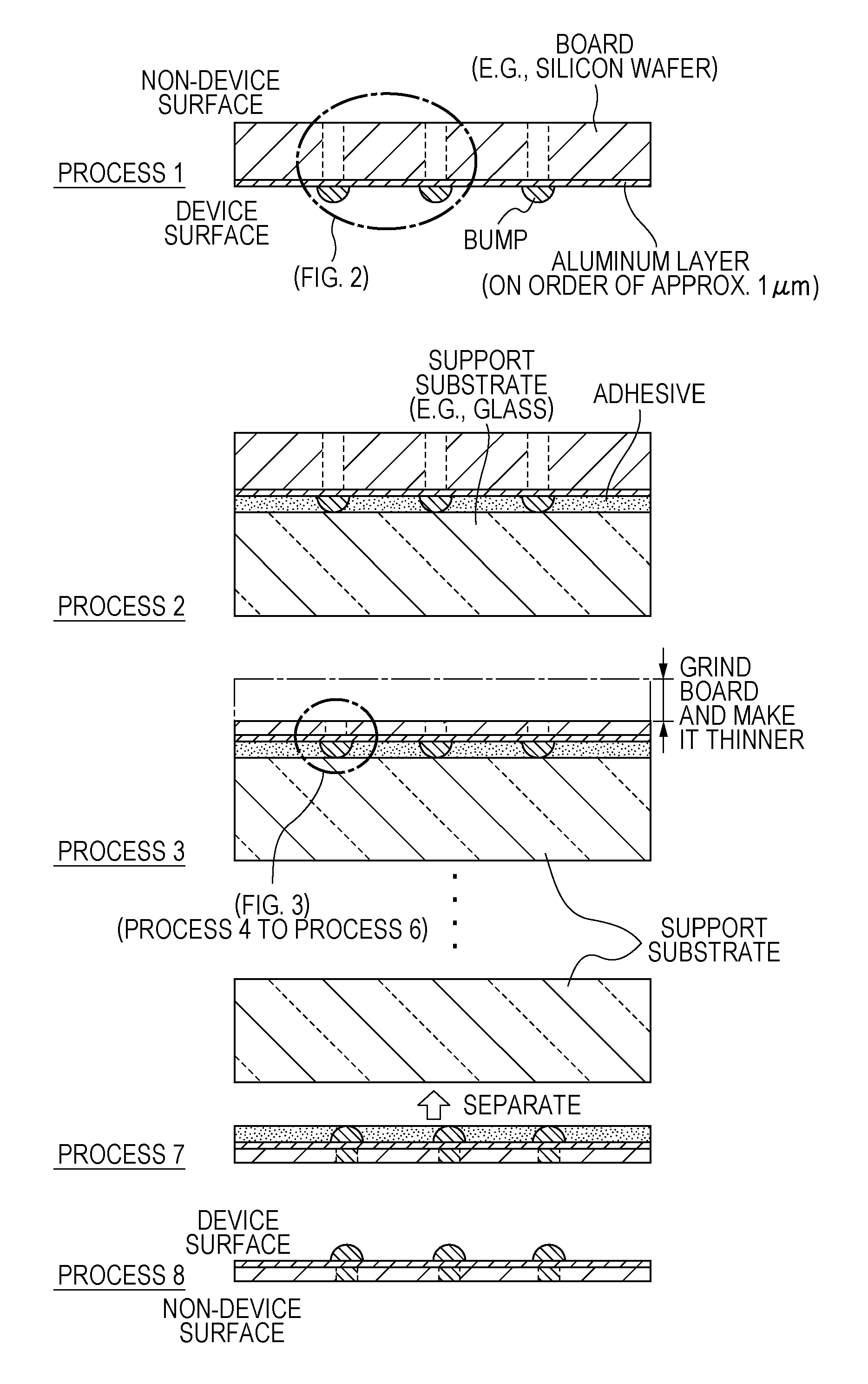
[0036]It should be understood that “ultrasound” or “ultrasonic wave” is a sound that is generally inaudible and that has a frequency of 20 kHz or more, and it is used in various technical applications, such as medical ultrasonic echo equipment, cleaners, fishfinders, and back sonar. In the embodiments of the present invention, it is assumed that a wave having a frequency of 20 kHz or more is used. In some cases, a pulsed wave containing wave components of different frequencies can be used.

[0037]The term “scanning” is movement of a location or space to be detected. In the present invention, it is moved over a two-dimensional range indicated by the XY directions or over a three-dimensional range indicated by the XYZ directions.

[0038]A first property of ultrasound is that the propagation velocity is significantly lower than that of a radio wave or other electromagnetic waves. The propagation velocity of ultrasound in a solid is higher than that in a liquid, the propagation velocity of ...


PUM


Abstract

A method and apparatus to detect a defect in a three-dimensional integrated structure by ultrasound scanning and to non-destructively detect the presence of a void that can occur in a process in a through silicon via (TSV) arranged in a board, such as a silicon wafer. To avoid measurement by ultrasound scanning over a board surface from being impeded by an object, such as a (solder) bump, scattering ultrasound, one or more TSVs belonging to a test element group (TEG) are selected from among a plurality of TSVs such that physical obstruction in the vicinity of the TEG.

Description

CROSS-REFERENCE TO RELATED APPLICATION[0001]This application claims priority under 35 U.S.C. §119 from Japanese Patent Application No. 2011-124548 filed Jun. 2, 2011, the entire contents of which are incorporated herein by reference.BACKGROUND OF THE INVENTION[0002]1. Field of the Invention[0003]The present invention relates to a technique for detecting a defect in a three-dimensional integrated structure by ultrasound scanning, and more specifically, it relates to non-destructive detection of the presence of a void that can occur in a process in a through silicon via (TSV) arranged in a board.[0004]2. Description of Related Art[0005]A three-dimensional integration technology using through silicon vias (TSVs) needs a technique for non-destructively detecting a defect in a TSV at an early stage in a process. One known method for producing a TSV is a “via last technique.” A through silicon via (TSV) can also be simply called “via.”[0006]FIG. 1 illustrates a general outline of processe...

Claims


Application Information

Patent Timeline
Patent Type & Authority Applications(United States)
IPC IPC(8): G01N29/04H01L23/48
CPCH01L21/76898G01N29/0681H01L2224/05647H01L2224/05624G01N29/11G01N2291/2697H01L22/12H01L22/20H01L22/34H01L2224/131H01L2224/0401H01L24/05H01L24/13H01L2924/00014H01L2924/014
Inventor HORIBE, AKIHIROYAMADA, FUMIAKI
Owner IBM CORP
Features
  • R&D
  • Intellectual Property
  • Life Sciences
  • Materials
  • Tech Scout
  • Unparalleled Data Quality
  • Higher Quality Content
  • 60% Fewer Hallucinations
Learn More