NAND structure and method of manufacturing the same

Inactive Publication Date: 2012-12-20
INST OF MICROELECTRONICS CHINESE ACAD OF SCI
View PDF6 Cites 25 Cited by
  • Summary
  • Abstract
  • Description
  • Claims
  • Application Information

AI Technical Summary

Benefits of technology

[0004]The present invention aims to solve at least one of the technical defects mentioned above, especially, to dim

Problems solved by technology

The problem of the prior art is that, with the need of small-sized digital devices, the requirements to the size and storage capacit

Method used


Image

  • NAND structure and method of manufacturing the same
  • NAND structure and method of manufacturing the same
  • NAND structure and method of manufacturing the same

Examples


Embodiment Construction

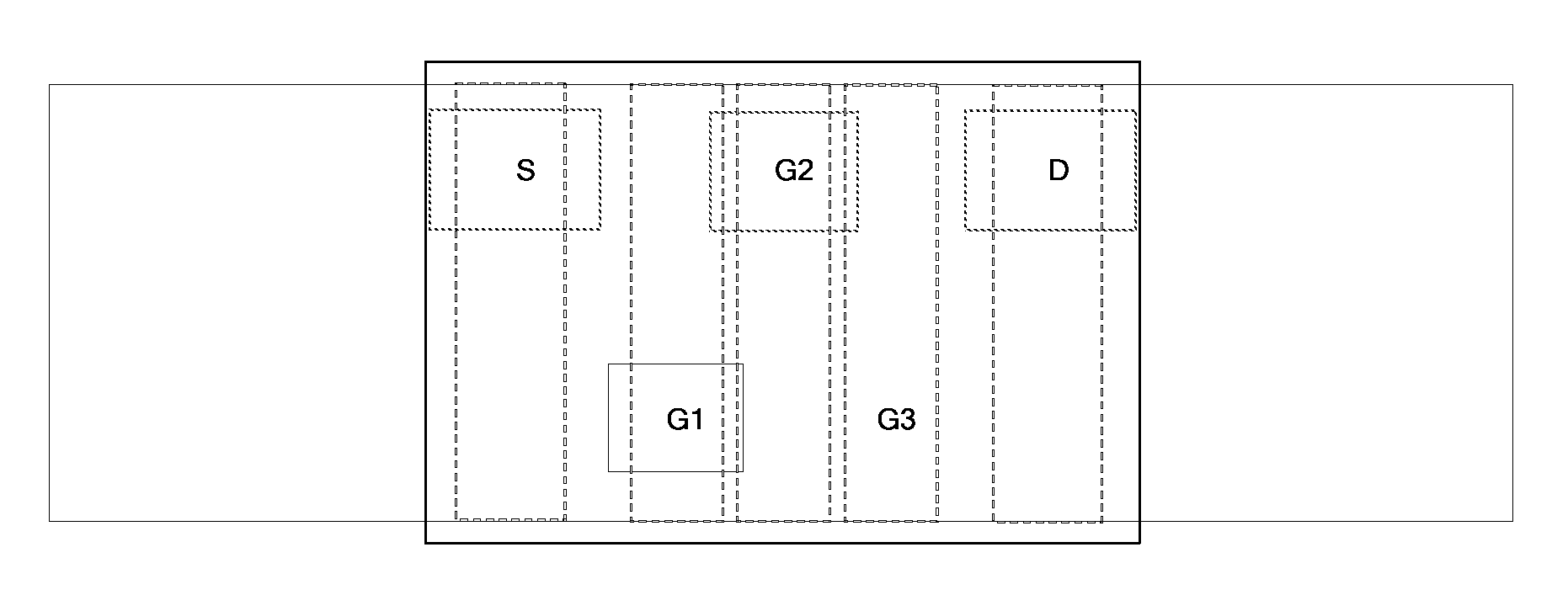
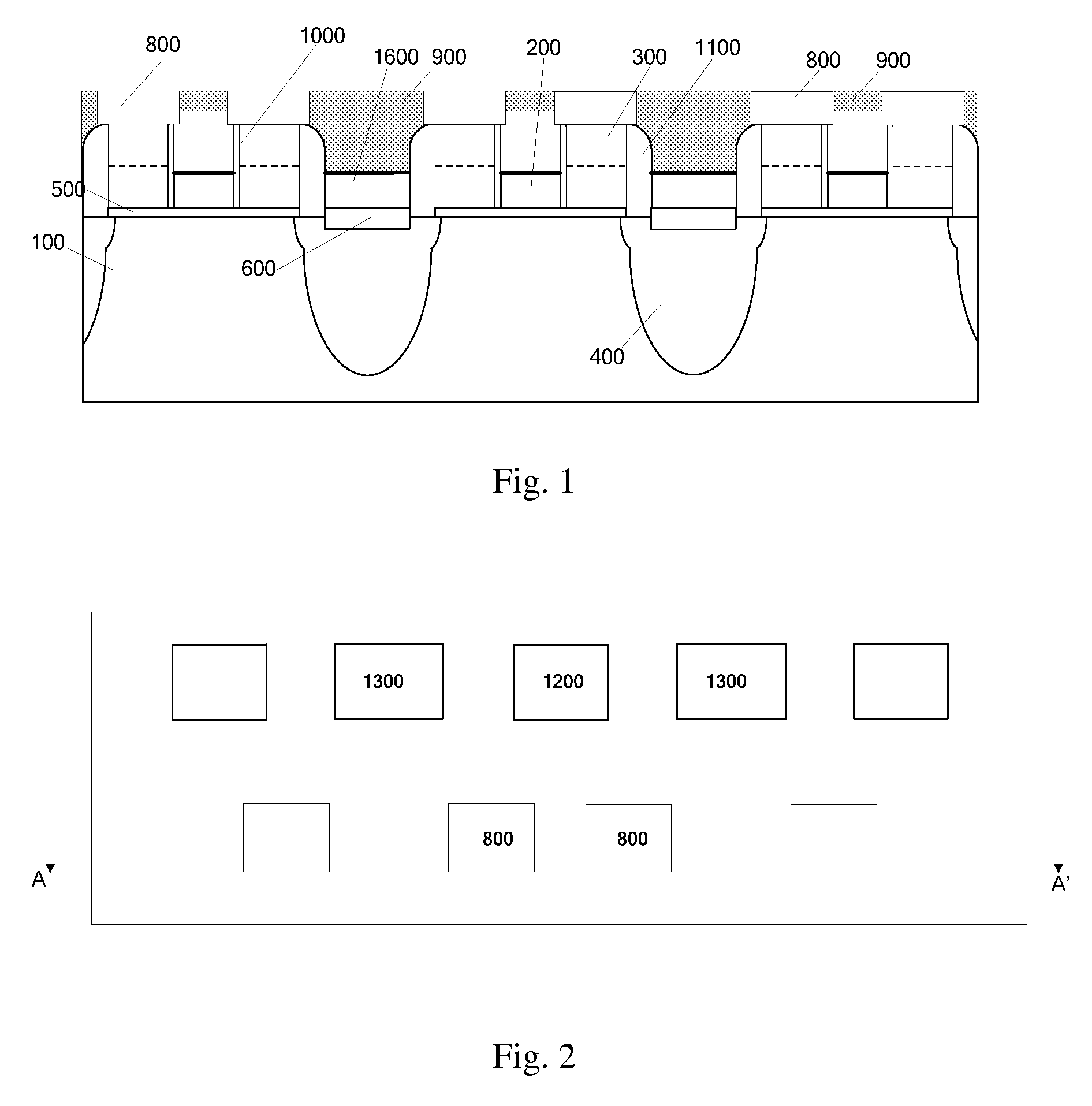
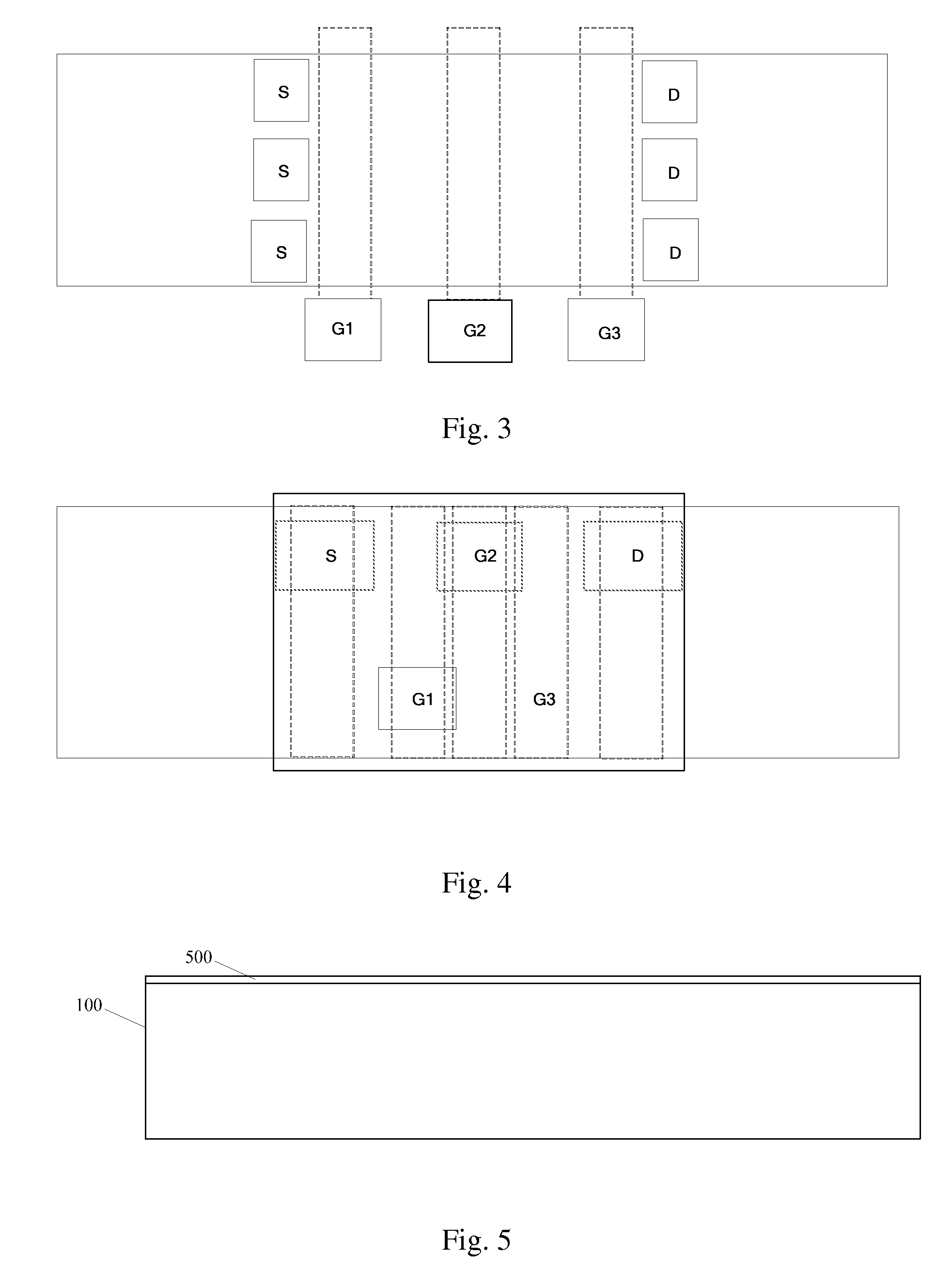
[0034]The embodiments of the present invention will be described in detail as follows and the examples therein will be illustrated in the drawings, wherein, from beginning to end, identical or similar reference numbers represent identical or similar element or elements having identical or similar functions. The following embodiments described with reference to the drawings are illustrative and only used to explain the present invention, but may not be interpreted as the restrictions of this invention.

[0035]The following disclosure provides a plurality of different embodiments or examples to achieve different structures of the present invention. To simplify the disclosure of the present invention, description of the components and arrangements of specific examples is given below. Of course, they are only illustrative and not limiting the present invention. Moreover, in the present invention, reference numbers and / or letters may be repeated in different embodiments. Such repetition is...


PUM


Abstract

The present invention provides a NAND gate structure, comprising: a substrate; a gate insulation layer formed on the substrate; a source/drain region formed in the substrate; a middle gate formed on the gate insulator layer, a first gate and a second gate on each side of the middle gate, first sidewall spacers between the first gate and the middle gate and between the second gate and the middle gate, and second sidewall spacers outside the first gate and the second gate, wherein, a first contact hole region is provided on the middle gate, second contact hole regions are provided respectively on the first gate and the second gate, and the first contact hole region and the second contact hole regions are in staggered arrangement. The present invention proposes a new NAND structure and a method of manufacturing the same. With the NAND structure, about 30-50% area of the chip may be effectively reduced.

Description

FIELD OF THE INVENTION[0001]The present invention relates to the technical field of semiconductor design and manufacture, and particularly, relates to a self-aligned small size NAND structure and a method of manufacturing the same.BACKGROUND OF THE INVENTION[0002]NAND structure is commonly used in flash memory, and NAND flash memory is better than Hard Disk Drive. As people are continuing to pursue products of lower power consumption, less weight but better performance, NAND is widely used because it has the advantages of higher cell density, higher storage density, faster write and erase speed, and so forth. Having a cell size almost only half of that of a NOR device cell, NAND flash memory can provide higher capacity than NOR device in a given mould size and has very fast write and erase speed. The main function of NAND flash memory is for data storage. At present, it is mainly used in flash memory cards of, for example, digital camera etc., and MP3 players.[0003]The problem of th...

Claims


Application Information

Patent Timeline
IPC IPC(8): H01L29/78H01L21/336
CPCH01L27/11519H01L27/11524H01L27/11521H10B41/10H10B41/35H10B41/30
Inventor LIANG, QINGQINGZHONG, HUICAIZHU, HUILONG
Owner INST OF MICROELECTRONICS CHINESE ACAD OF SCI
Why Eureka
Try Eureka