Multilayer graphene and power storage device

a power storage device and graphene technology, applied in cell components, applications, transportation and packaging, etc., can solve the problems of electrode deformation, broken electrodes, difficult ions to be transferred in the direction perpendicular to the graphene, etc., to increase the amount of active materials, reduce the amount of binder, and increase the effect of durability

Inactive Publication Date: 2012-12-27
SEMICON ENERGY LAB CO LTD
View PDF4 Cites 57 Cited by
  • Summary
  • Abstract
  • Description
  • Claims
  • Application Information

AI Technical Summary

Benefits of technology

[0022]Thus, the positive electrode active material layer and the negative electrode active material layer contain multilayer graphenes, whereby the amounts of binder and conductive additives which are contained in the positive electrode active material layer and the negative electrode active material layer can be reduced; accordingly, the amount of active materials contained in the positive electrode active material layer and the negative electrode active material layer can be increased. Further, the reduction in amount of the binder leads to an increase in durability of the positive electrode active material layer and the negative electrode active material layer.
[0023]According to one embodiment of the present invention, a surface of an uneven active material in a positive electrode or a negative electrode of a power storage device is coated with multilayer graphene. As w...

Problems solved by technology

However, the transfer of ions in the direction perpendicular to the graphene is difficult.
Further, the binder included in the ...

Method used


Image

  • Multilayer graphene and power storage device
  • Multilayer graphene and power storage device
  • Multilayer graphene and power storage device

Examples


embodiment 1

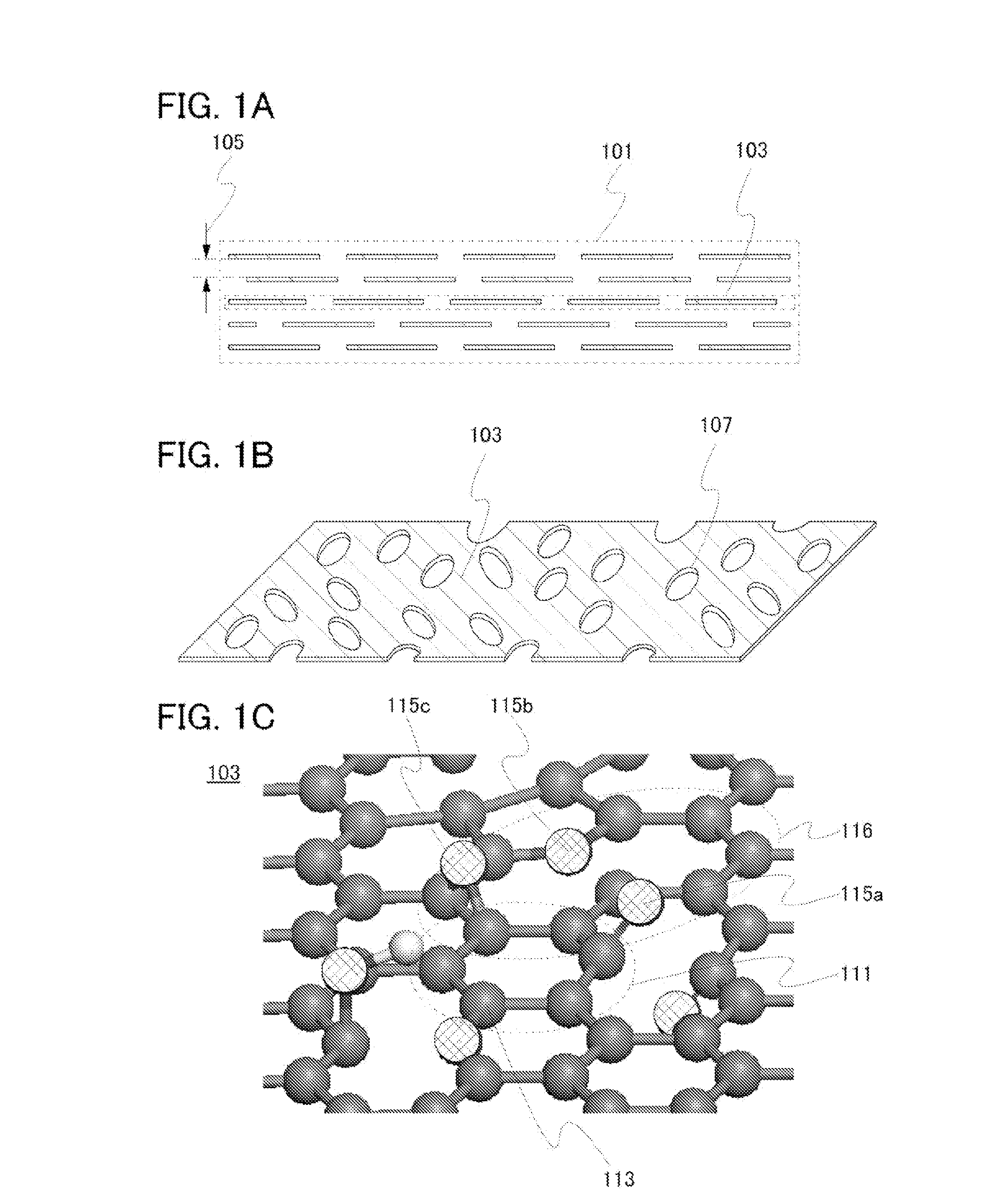
[0035]In this embodiment, a structure of multilayer graphene and a formation method thereof will be described with reference to FIGS. 1A to 1C.

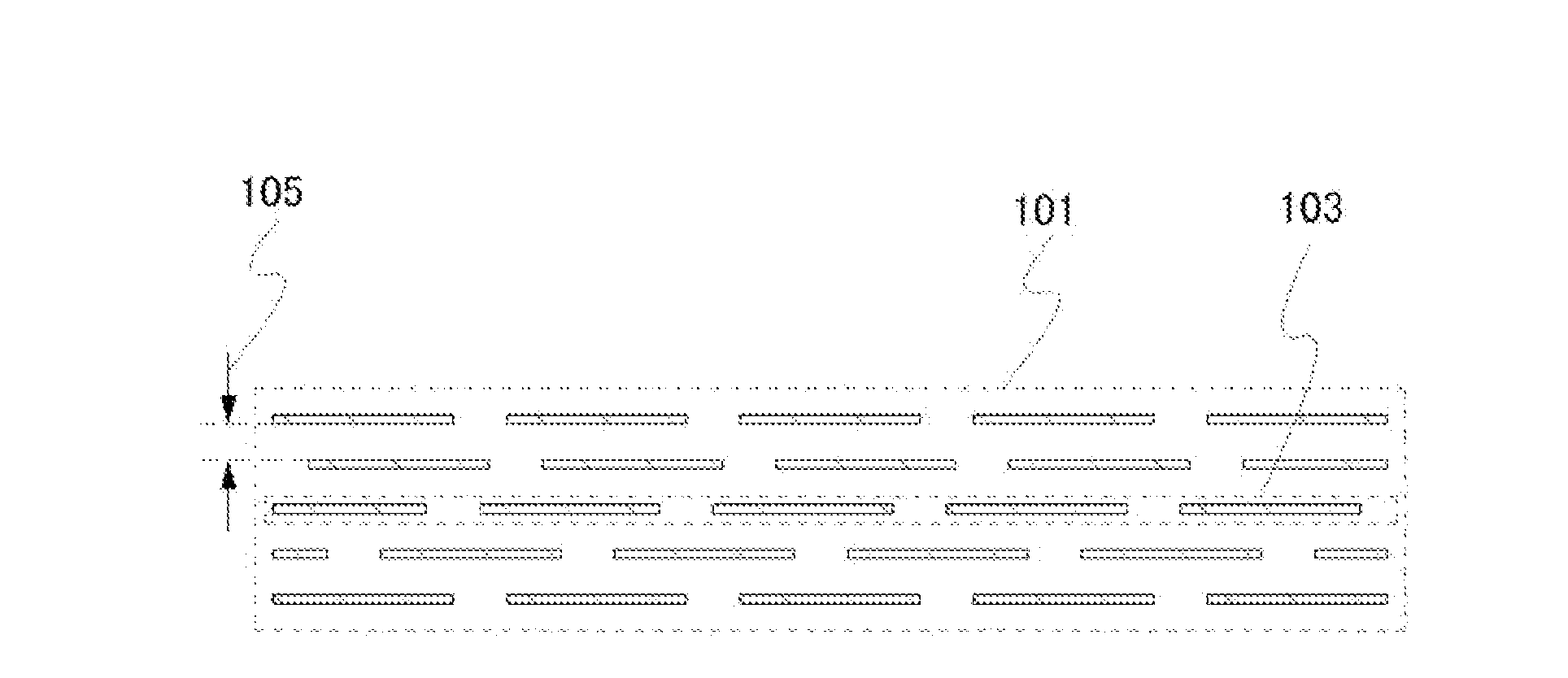
[0036]FIG. 1A is a cross-sectional schematic view of multilayer graphene 101. In the multilayer graphene 101, a plurality of graphenes 103 overlap with each other in parallel or in substantially parallel. An interlayer distance 105 between the graphenes in this case is greater than 0.34 nm and less than or equal to 0.5 nm, preferably greater than or equal to 0.38 nm and less than or equal to 0.42 nm, more preferably greater than or equal to 0.39 nm and less than or equal to 0.41 nm. The multilayer graphene 101 includes two or more and 100 or less layers of the grahenes 103.

[0037]FIG. 1B is a perspective view of the graphene 103 in FIG. 1A. The graphene 103 has a sheet-like shape several μm on a side and includes openings 107. The openings 107 serve as paths which allow the transfer of ions. Thus, in the multilayer graphene 101 in FIG. 1A, ion...

embodiment 2

[0051]In this embodiment, a structure of an electrode of a power storage device and a formation method of the electrode will be described.

[0052]First, a negative electrode and a formation method thereof will be described.

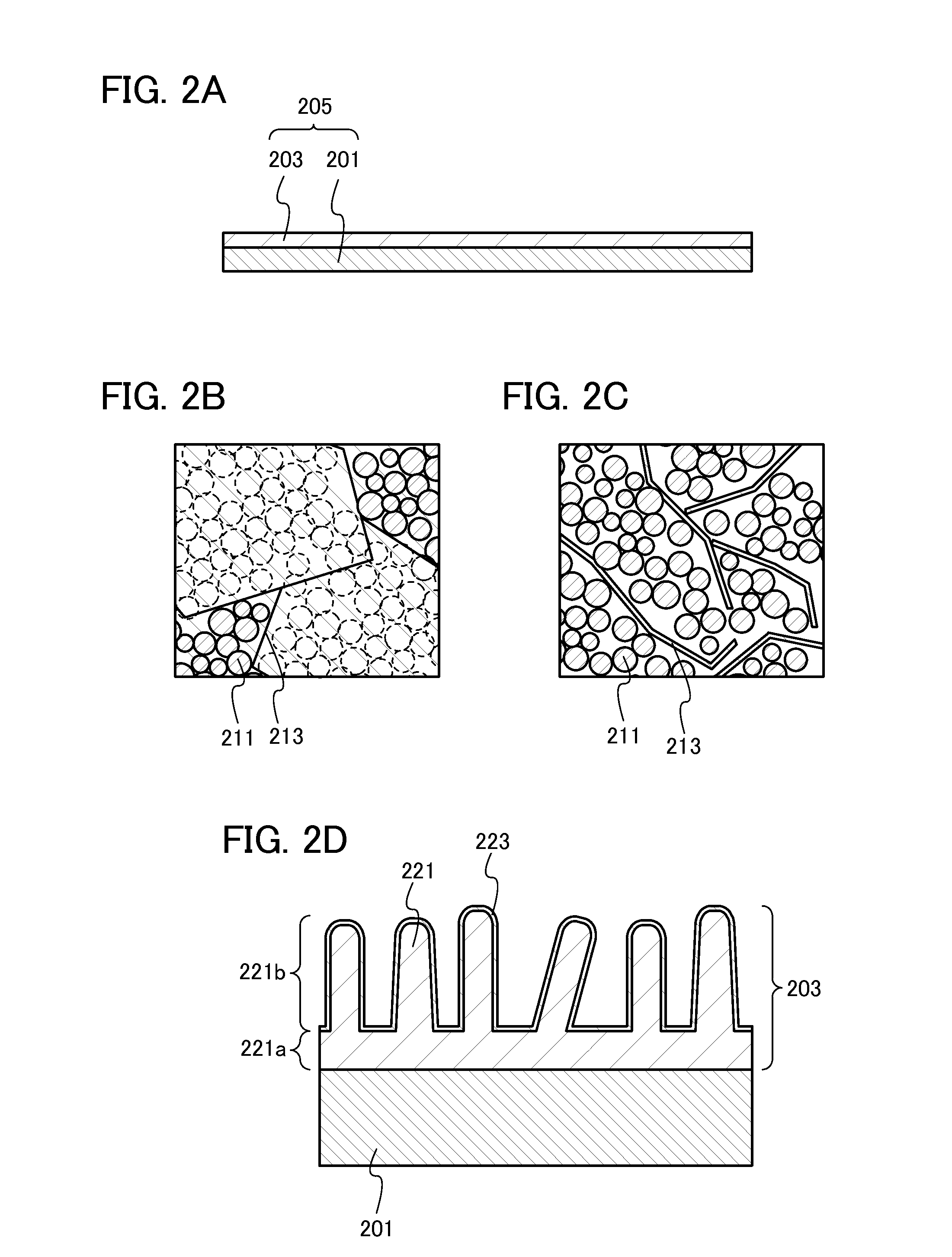
[0053]FIG. 2A is a cross-sectional view of a negative electrode 205. In the negative electrode 205, a negative electrode active material layer 203 is formed over a negative electrode current collector 201.

[0054]Note that an active material refers to a material that relates to intercalation and deintercalation of ions serving as carriers. Thus, the active material and the active material layer are distinguished.

[0055]As the negative electrode current collector 201, a material having high conductivity such as copper, stainless steel, iron, or nickel can be used. The negative electrode current collector 201 can have a foil shape, a plate shape, a film shape, or the like as appropriate.

[0056]The negative electrode active material layer 203 is formed using a negative ele...

embodiment 3

[0096]In this embodiment, a method for manufacturing a power storage device will be described.

[0097]A lithium-ion secondary battery in this embodiment which is a typical example of power storage devices will be described with reference to FIG. 4. Here, description will be given below of a cross-sectional structure of the lithium-ion secondary battery.

[0098]FIG. 4 is a cross-sectional view of the lithium ion secondary battery.

[0099]A lithium-ion secondary battery 400 includes a negative electrode 411 including a negative electrode current collector 407 and a negative electrode active material layer 409, a positive electrode 405 including a positive electrode current collector 401 and a positive electrode active material layer 403, and a separator 413 provided between the negative electrode 411 and the positive electrode 405. Note that the separator 413 is impregnated with an electrolyte 415. The negative electrode current collector 407 is connected to an external terminal 419 and the...


PUM


Abstract

To provide graphene through which ions can transfer in the direction perpendicular to a plane of the graphene. Multilayer graphene includes a plurality of graphenes stacked in a layered manner. The plurality of graphenes contain a six-membered ring composed of carbon atoms, a poly-membered ring which is a seven or more-membered ring composed of carbon atoms or carbon atoms and one or more oxygen atoms, and an oxygen atom bonded to one of the carbon atoms in the six-membered ring and the poly-membered ring, which is a seven or more-membered ring. The interlayer distance between adjacent graphenes of the plurality of graphenes is greater than 0.34 nm and less than or equal to 0.5 nm, preferably greater than or equal to 0.38 nm and less than or equal to 0.42 nm.

Description

BACKGROUND OF THE INVENTION[0001]1. Field of the Invention[0002]The present invention relates to multilayer graphene, a power storage device containing the multilayer graphene, and a semiconductor device containing the multilayer graphene.[0003]2. Description of the Related Art[0004]In recent years, the use of graphene as a conductive electronic material in semiconductor devices has been studied. Graphene is a lateral layer in graphite, i.e., a carbon layer in which six-membered rings each composed of carbon atoms are connected in the planar direction, and a stack of two or more and 100 or less carbon layers is referred to as multilayer graphene.[0005]Graphene is chemically stable and has favorable electric characteristics and thus has been expected to be applied to channel regions of transistors, vias, wirings, and the like included in semiconductor devices.[0006]On the other hand, an active electrode material is coated with graphene in order to increase the conductivity of a mater...

Claims


Application Information

Patent Timeline
IPC IPC(8): B32B5/00H01M4/62B82Y30/00
CPCH01M4/625B82Y40/00B82Y30/00C01B31/0476C01P2004/04C01P2004/03C01B32/192Y10T428/249921Y02E60/10
Inventor OGUNI, TEPPEITODORIKI, HIROATSUOSADA, TAKESHI
Owner SEMICON ENERGY LAB CO LTD
Why Eureka
Try Eureka