
Nonvolatile semiconductor memory device

a semiconductor memory and non-volatile technology, applied in the field of non-volatile semiconductor memory devices, can solve the problems of high probability of occurrence of erroneous reads and high deterioration amount, and achieve the effect of reducing the voltage tolerance, reducing the circuit area, and reducing the drive circuit for bit line selective transistors

Active Publication Date: 2013-01-03
PANASONIC SEMICON SOLUTIONS CO LTD
View PDF5 Cites 0 Cited by
  • Summary
  • Abstract
  • Description
  • Claims
  • Application Information

AI Technical Summary

Benefits of technology

The present patent aims to provide a nonvolatile semiconductor memory device with a reduced circuit area. This is achieved by using a virtual ground and reducing the number of drive circuits for bit line selective transistors. The first and second bit lines connected to each nonvolatile memory cell are respectively selected by the first and second selective transistor groups, with separate drive circuits for each group. This allows for independent setting of voltages for driving the gates of each group, leading to a smaller circuit area and use of transistors lower in voltage tolerance.

Problems solved by technology

The reason is that, when two-bit information is stored in one memory cell, the probability of occurrence of erroneous read is high, compared with the case of storing one-bit information, due to decrease in Vt difference between the “0” state and the “1” state and increase in Vt deterioration amount caused by retention, etc.

Method used


Image

  • Nonvolatile semiconductor memory device
  • Nonvolatile semiconductor memory device
  • Nonvolatile semiconductor memory device

Examples


first embodiment

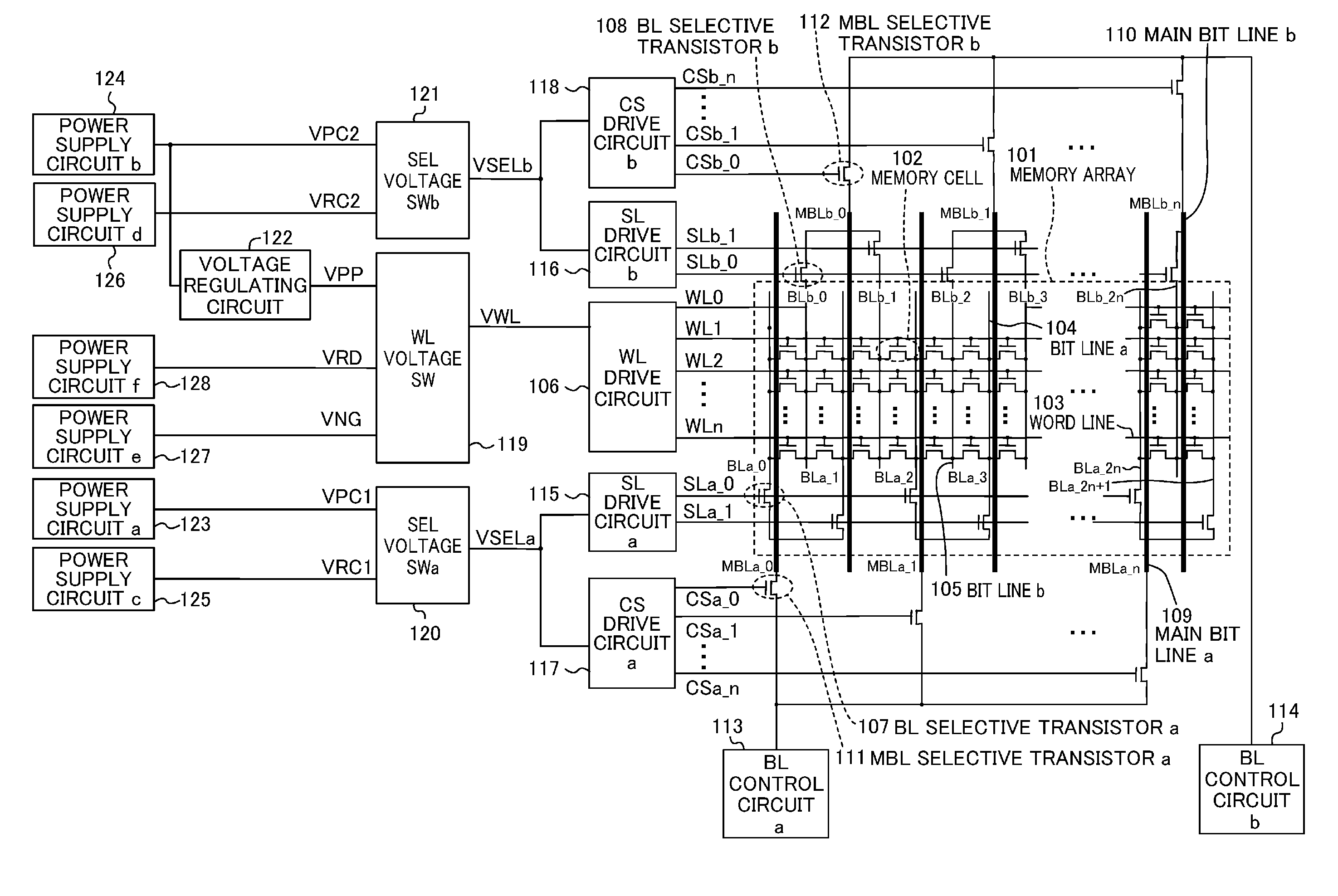
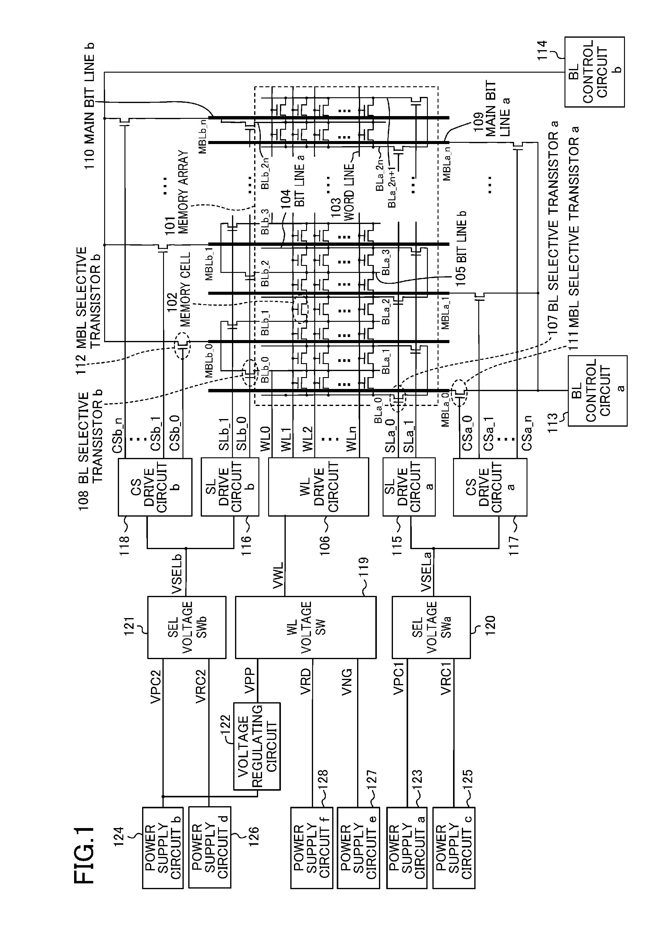
[0022]FIG. 1 is a view showing a configuration of a nonvolatile semiconductor memory device of the first embodiment. In FIG. 1, a memory array 101 includes: a plurality of nonvolatile memory cells 102 arranged in the X and Y directions into an array; a plurality of word lines 103 (WL0 to WLn) extending in the X direction in the region of arrangement of the memory cells 102; and a plurality of bit lines a 104 (BLa_0 to BLa_2n+1) as the first bit lines and a plurality of bit lines b 105 (BLb_0 to BLb_2n) as the second bit lines extending in the Y direction in the region of arrangement of the memory cells 102. The memory cells 102, the word lines 103, the bit lines a 104, and the bit lines b 105 are arranged using a virtual ground.

[0023]It is herein assumed that the memory cells 102 are metal oxide nitride oxide silicon (MONOS) memory cells that store information by local injection of charge. To each of the memory cells 102, connected are the word line 103 for control of the gate, the ...

second embodiment

[0050]FIG. 3 is a view showing a configuration of a nonvolatile semiconductor memory device of the second embodiment. In FIG. 3, components common to those in FIG. 1 are denoted by the same reference characters, and detailed description of such components is omitted here.

[0051]In the configuration of FIG. 3, the kinds and connection of the power supply circuits for supplying voltages to the SEL voltage switch a 120 and the SEL voltage switch b 121 are different from those in FIG. 1. That is, while the SEL voltage switch a 120 receives the voltage VPC1 supplied from the power supply circuit a 123 and the voltage VRC1 supplied from the power supply circuit c 125 in the configuration of FIG. 1, the power supply circuit a 123 is omitted and the SEL voltage switch a 120 receives the voltage VRD supplied from the power supply circuit f 128 for the word line voltage for reading, in place of the voltage VPC1, in the configuration of FIG. 3. Also, while the SEL voltage switch b 121 receives ...


PUM


Abstract

Bit lines connected to each nonvolatile memory cell are selected by corresponding selective transistors. A first drive circuit for driving the gate of one of the selective transistors receives a voltage selected by a first voltage switch, and a second drive circuit for driving the gate of the other selective transistor receives a voltage selected by a second voltage switch. A transistor constituting the first drive circuit is different in structure from a transistor constituting the second drive circuit.

Description

CROSS-REFERENCE TO RELATED APPLICATION[0001]This is a continuation of PCT International Application PCT / JP2011 / 000360 filed on Jan. 24, 2011, which claims priority to Japanese Patent Application No. 2010-053247 filed on Mar. 10, 2010. The disclosures of these applications including the specifications, the drawings, and the claims are hereby incorporated by reference in their entirety.BACKGROUND[0002]The present disclosure relates to a nonvolatile semiconductor memory device having a memory array in which nonvolatile memory cells are arranged using a virtual ground.[0003]Flash electrically erasable nonvolatile semiconductor memory devices have a feature that stored information is not lost even in a power-off state. Various methods have been proposed on how to form an array of memory cells in a nonvolatile semiconductor memory device. Among such methods, there is a method where metal oxide nitride oxide silicon (MONOS) memory cells that store information by local injection of charge a...

Claims


Application Information

Patent Timeline
Patent Type & Authority Applications(United States)
IPC IPC(8): G11C16/12G11C16/04
CPCG11C16/0408G11C16/0491G11C16/10G11C16/0475G11C16/06
Inventor NAKAYAMA, MASAYOSHIONO, TAKASHIMOCHIDA, REIJI
Owner PANASONIC SEMICON SOLUTIONS CO LTD
Learn More