Mosfet and method for manufacturing the same

Active Publication Date: 2013-01-10
INST OF MICROELECTRONICS CHINESE ACAD OF SCI
View PDF11 Cites 8 Cited by
  • Summary
  • Abstract
  • Description
  • Claims
  • Application Information

AI Technical Summary

Benefits of technology

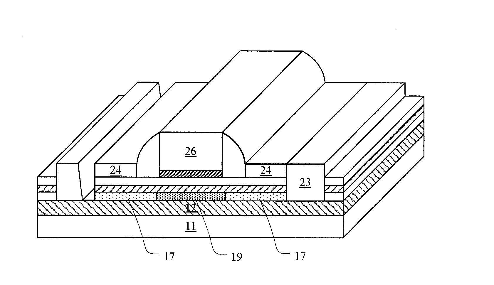
The present patent aims to provide a MOSFET that can adjust its threshold voltage and reduce leakage current between source / drain regions using a back gate. The back gate is connected to external circuits and applies a non-uniform voltage to the channel region through a buried insulating layer, improving the suppression of short channel effects. Additionally, the form of the back gate as a PNP or NPN junction prevents the formation of a conductive path and decreases leakage current.

Problems solved by technology

However, it is well known that short channel effects arise as the size of MOSFETs decreases.
However, in the above conventional SOI MOSFET, the back gate is mainly used for increasing the threshold voltage of the device, and the back gate cannot be used for adjusting the threshold voltage flexibly.
Furthermore, the MOSFETs may be damaged due to short circuit between source / drain regions via the back gate.

Method used


Image

  • Mosfet and method for manufacturing the same
  • Mosfet and method for manufacturing the same
  • Mosfet and method for manufacturing the same

Examples


Embodiment Construction

[0020]Exemplary embodiments of the present disclosure will be described in more details below with reference to the accompanying drawings. In the drawings, like reference numerals denote like members. The figures are not drawn to scale, for the sake of clarity.

[0021]Some particular details of the present disclosure will be described below, such as exemplary semiconductor structures, materials, dimensions, process steps and technologies of the semiconductor device, for better understanding of the present disclosure. However, it can be understood by one skilled person in the art that these details are not always essential for but can be varied in a specific implementation of the disclosure. Unless the context clearly indicates otherwise, each part of the semiconductor device can be made of material(s) well known to one skilled person in the art.

[0022]In the present application, the term “semiconductor structure” means generally the whole semiconductor structure formed at each step of ...


PUM


Abstract

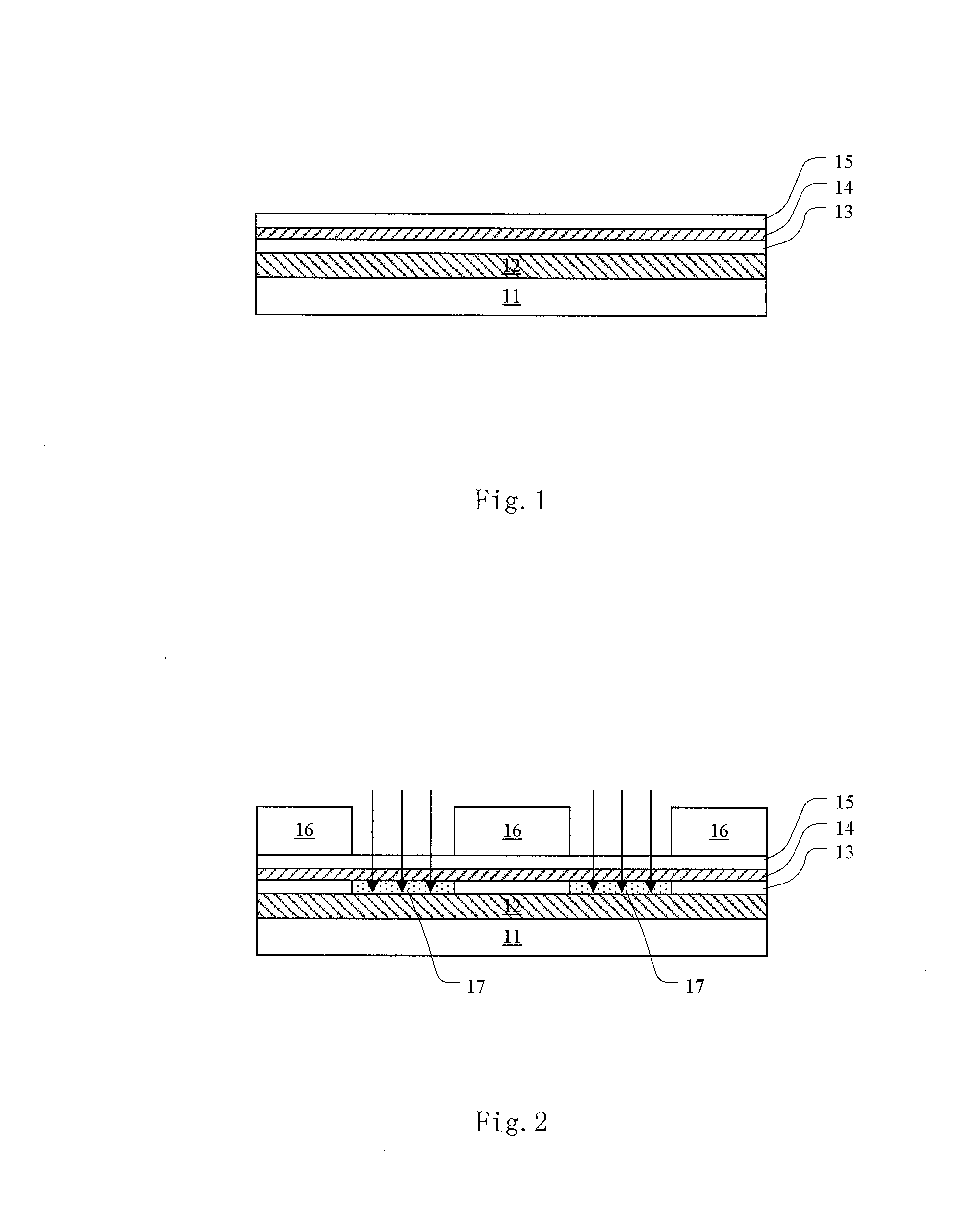
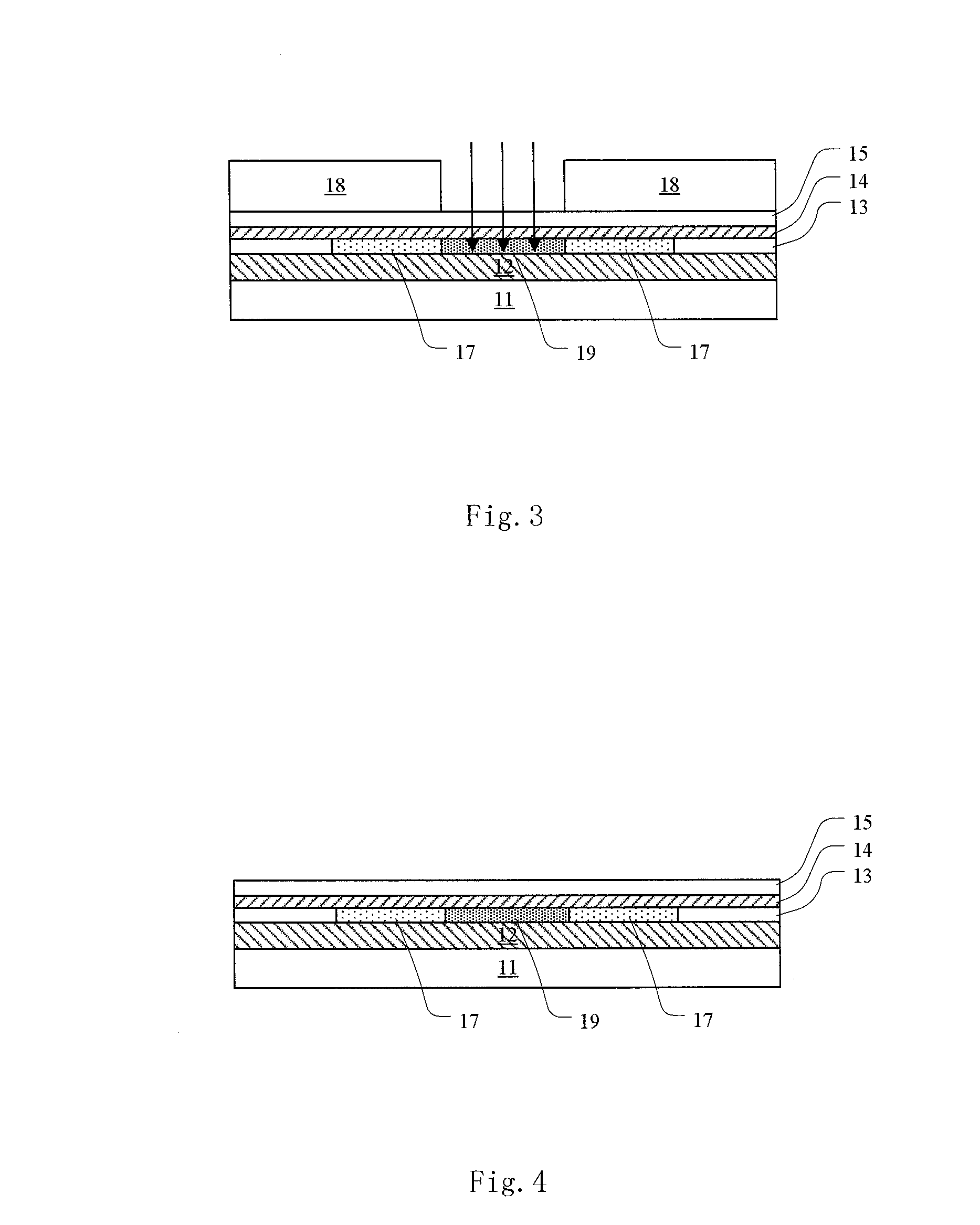
The present application discloses an MOSFET and a method for manufacturing the same. The MOSFET comprises: a semiconductor substrate; a first insulation buried layer disposed on the semiconductor substrate; a back gate formed in a first semiconductor layer which is disposed on the first insulation buried layer; a second insulation buried layer disposed on the first semiconductor layer; source / drain regions formed in a second semiconductor layer which is disposed on the second insulation buried layer; a gate disposed on the second semiconductor layer; and electric connections to the source / drain regions, the gate and the back gate, wherein the back gate comprises first back gate regions of a first conductivity type which are disposed under the source / drain regions and a second back gate region of a second conductivity type which is disposed under a channel region, the first back gate regions adjoins the second back gate region, the first conductivity type is opposite to the second conductivity type, and the electric connection to the back gate comprise a conductive via contacted with one of the first back gate regions. The MOSFET, of any conductivity type, can have adjustable threshold voltage and reduced leakage current via the back gate between the source / drain regions by using the back gate in the form of a PNP junction or an NPN junction.

Description

CROSS-REFERENCE TO RELATED APPLICATION[0001]This application claims priority to the Chinese Patent Application No. 201110189100.X, filed on Jul. 7, 2011, entitled “MOSFET AND METHOD FOR MANUFACTURING THE SAME”, which is incorporated herein by reference in its entirety.TECHNICAL FIELD[0002]The present disclosure relates to a MOSFET and a method for manufacturing the same, and in particular, to a MOSFET with a back gate and a method for manufacturing the same.BACKGROUND[0003]An important trend in development of semiconductor technology is scaling down of metal-oxide-semiconductor field effect transistors (MOSFETs) for improving integration level and reducing manufacturing cost. However, it is well known that short channel effects arise as the size of MOSFETs decreases. As the MOSFETs are scaled down, a gate also has a reduced effective length and actually controls fewer charges in a depletion region when a gate voltage is applied. Consequently, a threshold voltage of the MOSFETs drops...

Claims


Application Information

Patent Timeline
IPC IPC(8): H01L29/772H01L21/336
CPCH01L21/2652H01L29/78648H01L29/42384H01L21/2658
Inventor ZHU, HUILONGLIANG, QINGQINGLUO, ZHIJIONGYIN, HAIZHOU
Owner INST OF MICROELECTRONICS CHINESE ACAD OF SCI
Why Eureka
Try Eureka