Semiconductor device and manufacturing method thereof

Active Publication Date: 2013-01-24
SEMICONDUCTOR MANUFACTURING INTERNATIONAL (BEIJING) CORP
View PDF8 Cites 11 Cited by
  • Summary
  • Abstract
  • Description
  • Claims
  • Application Information

AI Technical Summary

Benefits of technology

The patent is about a semiconductor device with very thin regions called source / drain extension regions that have a high concentration of activated dopants. The method for making this device is also provided. The technical effect of this patent is to improve the performance of semiconductor devices by creating shallow junction depth and high activated dopant concentration in the source / drain extension regions.

Problems solved by technology

Incidentally, although SIMS (Secondary Ion Mass Spectrometry) is generally used to measure dopant profiles after laser melting / sub-melting annealing, SIMS is unable to distinguish whether dopants are activated or not.

Method used


Image

  • Semiconductor device and manufacturing method thereof
  • Semiconductor device and manufacturing method thereof
  • Semiconductor device and manufacturing method thereof

Examples


Embodiment Construction

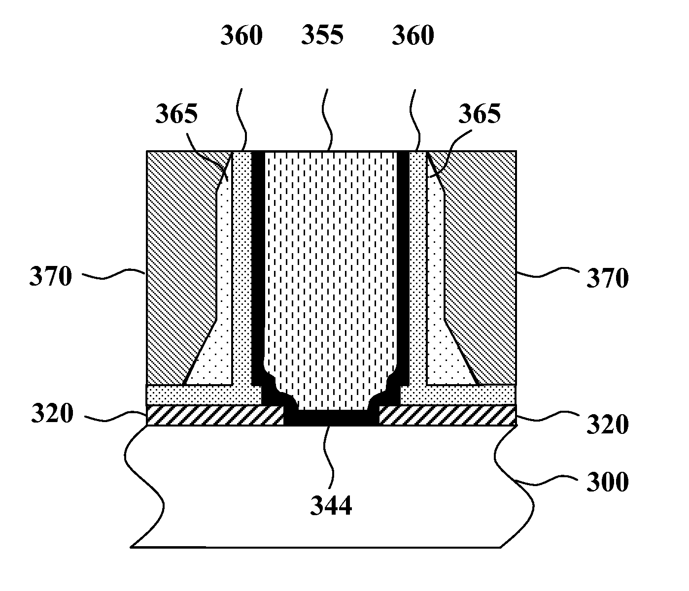
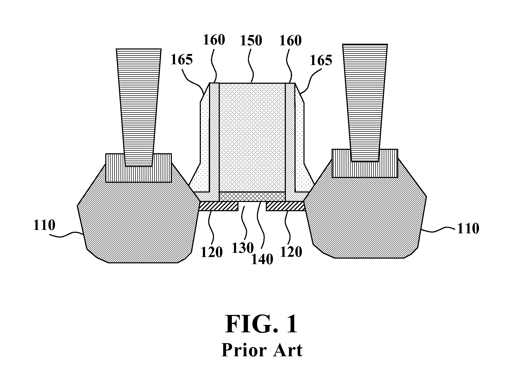
[0061]Exemplary embodiments of this disclosure will be described in detail below with reference to the accompanying drawings. It shall be noted that the following description is merely exemplary in nature. The components, steps and numerical values set forth in the embodiments do not limit the scope of this disclosure unless it is otherwise specifically stated. In addition, techniques, methods and devices known by persons skilled in the art may not be discussed in detail, but are intended to be a part of the specification where appropriate.

[0062]This disclosure will be described below by taking a transistor as an example. It is to be noted that, this disclosure is applicable not only to PMOS transistors, but also to NMOS transistors, namely, is applicable to CMOS transistors. In addition, this disclosure is also applicable to other semiconductor devices, including Replacement Gate (RMG) devices (such as finFET) and the like.

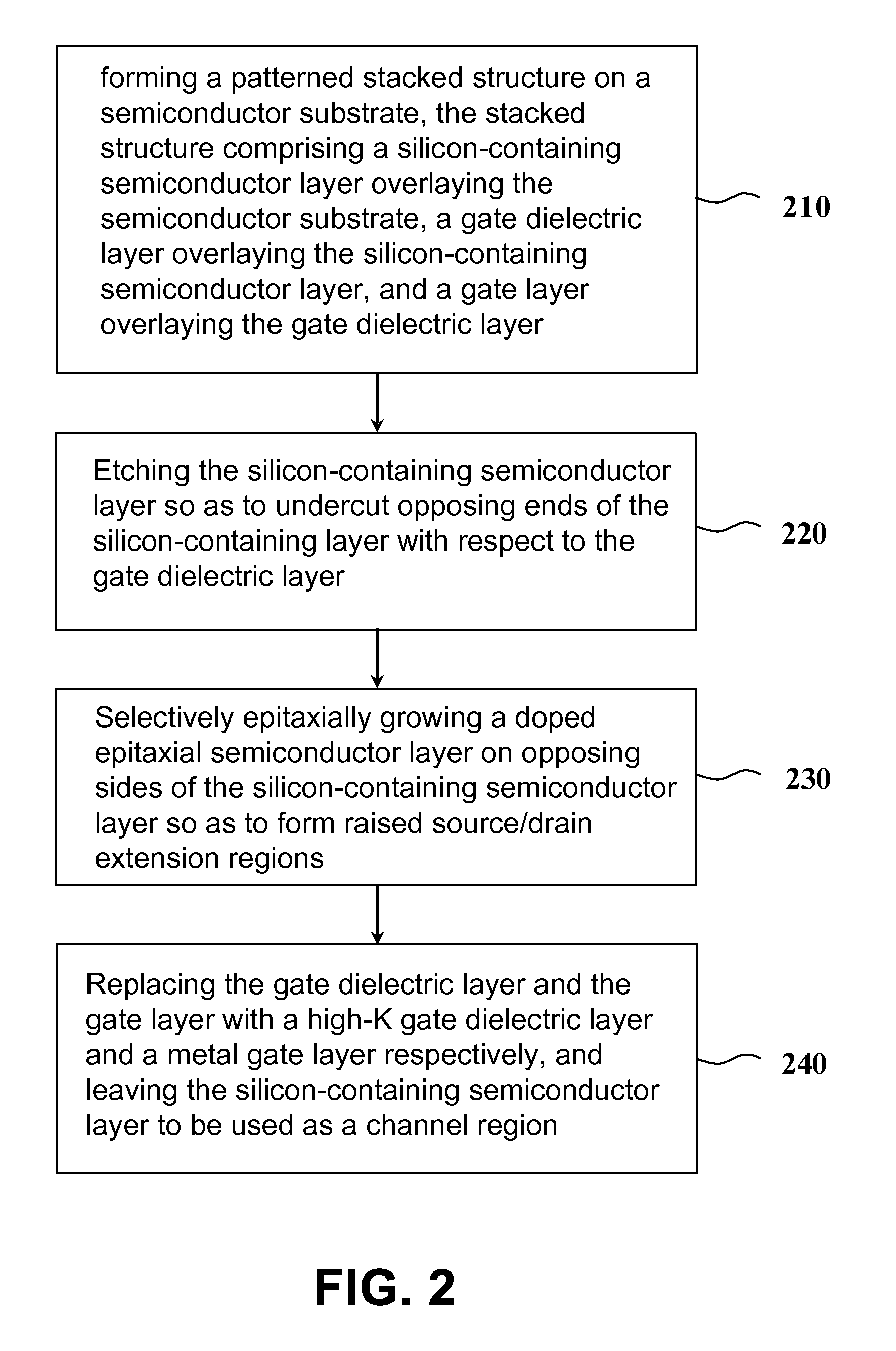
[0063]One embodiment of a manufacturing method of a semicon...


PUM


Abstract

This disclosure relates to a semiconductor device and a manufacturing method thereof. The semiconductor device comprises: a patterned stacked structure formed on a semiconductor substrate, the stacked structure comprising a silicon-containing semiconductor layer overlaying the semiconductor substrate, a gate dielectric layer overlaying the silicon-containing semiconductor layer and a gate layer overlaying the gate dielectric layer; and a doped epitaxial semiconductor layer on opposing sides of the silicon-containing semiconductor layer forming raised source / drain extension regions. Optionally, the silicon-containing semiconductor layer may be used as a channel region. According to this disclosure, the source / drain extension regions can be advantageously made to have a shallow junction depth (or a small thickness) and a high doping concentration.

Description

CROSS-REFERENCES TO RELATED APPLICATIONS[0001]This application claims priority to Chinese Patent Application No. 201110201414.7 filed on Jul. 19, 2011 and entitled “Semiconductor Device and Manufacturing Method thereof” and Chinese Patent Application No. 201110201273.9 filed on Jul. 19, 2011 and entitled “Semiconductor Device and Manufacturing Method Thereof”, which are incorporated herein by reference in their entirety.BACKGROUND OF THE INVENTION[0002]1. Field of the Invention[0003]This disclosure relates to a semiconductor device and a manufacturing method thereof. This disclosure in particular relates to a semiconductor device with epitaxial source / drain extension regions and a manufacturing method thereof.[0004]2. Description of the Related Art[0005]Nowadays, millions of semiconductor devices are integrated together to form very large scale integrated circuits.[0006]FIG. 1 shows a sectional view of a conventional semiconductor device (transistor). The transistor generally compri...

Claims


Application Information

Patent Timeline
IPC IPC(8): H01L29/78H01L21/336
CPCH01L29/41783H01L29/495H01L29/4966H01L29/517H01L29/66545H01L29/165H01L29/66621H01L29/66636H01L29/7833H01L29/7834H01L29/1054H01L29/6659
Inventor MIENO, FUMITAKE
Owner SEMICONDUCTOR MANUFACTURING INTERNATIONAL (BEIJING) CORP
Why Eureka
Try Eureka