N-FET with a Highly Doped Source/Drain and Strain Booster

a technology of source/drain and booster, which is applied in the direction of semiconductor devices, electrical equipment, basic electric elements, etc., can solve the problems of reducing transistor performance, affecting the drive current of the n-fet, and reducing so as to reduce the parasitic series source/drain resistance, increase the mobility of the carrier, and increase the drive current

Active Publication Date: 2010-06-24
TAIWAN SEMICON MFG CO LTD
View PDF19 Cites 72 Cited by
  • Summary
  • Abstract
  • Description
  • Claims
  • Application Information

AI Technical Summary

Benefits of technology

[0010]In accordance with an illustrative embodiment of the present invention, a method of making an N-type field effect transistor (N-FET) is presented. The method provides a substrate with a Ge channel region. A gate dielectric is formed over the Ge channel and a gate electrode is formed over the gate dielectric. Sacrificial gate spacers are disposed on the side walls of the gate dielectric and gate electrode. Cavities are etched into the substrate extending under the sacrificial gate spacers. Si1−xGex source / drain regions are doped in-situ during formation, x<0.85.
[0011]Advantages of preferred embodiments of the present invention include providing a high speed MOSFET with reduced parasitic series source / drain resistance (Rsd) and a shallow source / drain junction depth.
[0012]A further advantage is providing a tensile strain on the N-FET channel region thereby increasing carrier mobility, thus increasing drive current.

Problems solved by technology

However, dopant activation in source / drain regions may be an issue in current Ge MOSFETs, especially the N-type MOSFET or N-FET.
The external resistance may reduce transistor performance.
For instance, the drive current of the N-FET may be impacted negatively if the external resistance of the N-FET is high.
Further, a desired low value for drain induced barrier lowering (DIBL) may not be achieved in high external resistance N-FET structures.
Thus, there are challenges due to scaling planar bulk CMOS because of the high channel doping required to reduce the parasitic series source / drain resistance (Rsd) to acceptable values while employing shallow source / drain junction depth.

Method used


Image

  • N-FET with a Highly Doped Source/Drain and Strain Booster
  • N-FET with a Highly Doped Source/Drain and Strain Booster
  • N-FET with a Highly Doped Source/Drain and Strain Booster

Examples


Embodiment Construction

[0020]The making and using of the presently preferred embodiments are discussed in detail below. It should be appreciated, however, that an illustrative embodiment provides many applicable inventive concepts that can be embodied in a wide variety of specific contexts. The specific embodiments discussed are merely illustrative of specific ways to make and use the invention, and do not limit the scope of the invention.

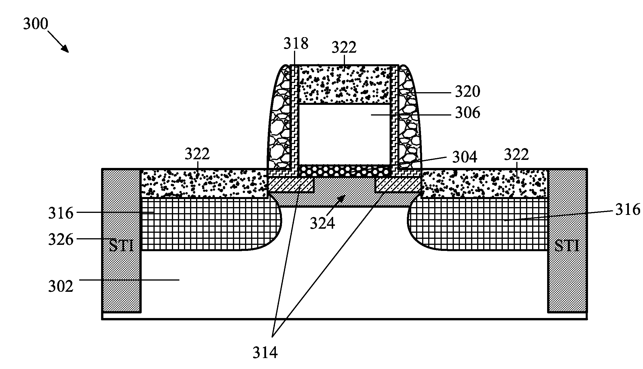
[0021]The present invention will be described with respect to illustrative embodiments in a specific context, namely a semiconductor device having a Ge N-FET with a highly doped source / drain and strain booster. The invention may also be applied, however, to other semiconductor devices.

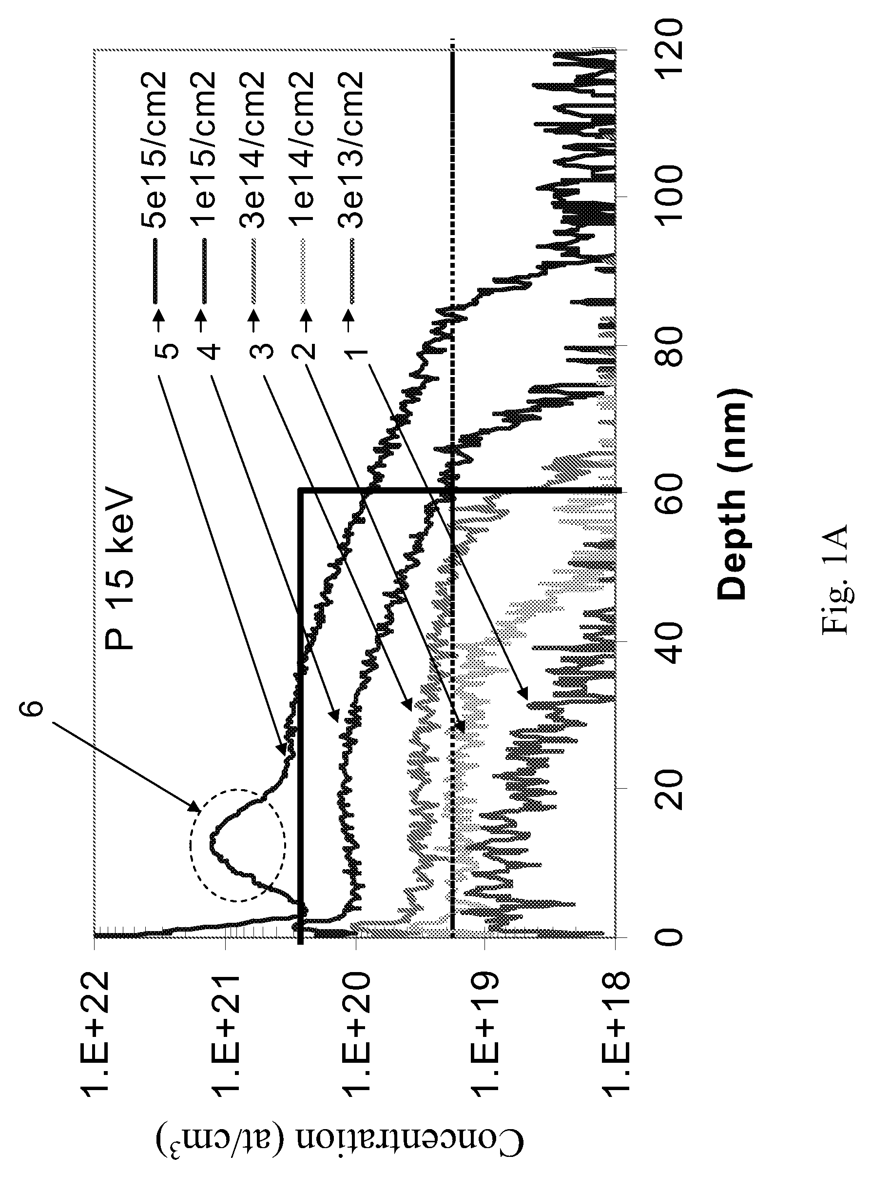
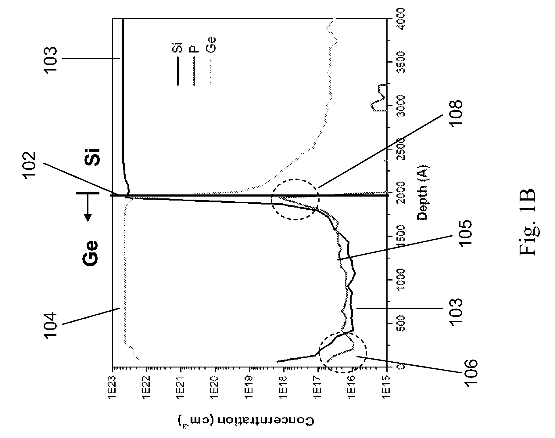
[0022]With reference now to FIG. 1a, a graph of phosphorous concentration versus depth for an implanted substrate is shown. FIG. 1b is a graph illustrating the phosphorous concentration in a multi-layer Ge and Si structure. FIG. 1c is a graph of phosphorous concentration in a SiGe layer.

[00...


PUM


Abstract

A structure and method of making an N-FET with a highly doped source/drain and strain booster are presented. The method provides a substrate with a Ge channel region. A gate dielectric is formed over the Ge channel and a gate electrode is formed over the gate dielectric. Sacrificial gate spacers are disposed on the sidewalls of the gate dielectric and gate electrode. Cavities are etched into the substrate extending under the sacrificial gate spacers. Si1−xGex source/drain regions are doped in-situ during formation, x<0.85.

Description

TECHNICAL FIELD[0001]The present invention relates generally to the manufacturing of semiconductor devices, and more particularly to a structure and method of making an N-FET with a highly doped source / drain and strain booster.BACKGROUND[0002]An important goal for the semiconductor industry is decreasing the size of semiconductor devices while increasing semiconductor performance. Planar transistors, such as metal oxide semiconductor field effect transistors (MOSFETs), are well suited for use in high-density integrated circuits (ICs).[0003]Higher speed MOSFETs can be formed using strained device technology. One manufacturing method involves epitaxial growth of silicon on top of a relaxed silicon-germanium under layer. Tensile strain is induced in the silicon as the lattice of the silicon layer is stretched to mimic the larger lattice constant of the underlying silicon-germanium. Conversely, compressive strain could be induced by using a solid solution with a smaller lattice constant...

Claims


Application Information

Patent Timeline
Patent Type & Authority Applications(United States)
IPC IPC(8): H01L29/78H01L21/336
CPCH01L21/26586H01L21/28255H01L29/7848H01L29/66477H01L29/7833H01L29/51
Inventor LIN, JING-CHENGYU, CHEN-HUA
Owner TAIWAN SEMICON MFG CO LTD
Why Eureka
Try Eureka