Semiconductor device and method for manufacturing the same

Inactive Publication Date: 2011-01-06
HITACHI LTD
View PDF6 Cites 10 Cited by
  • Summary
  • Abstract
  • Description
  • Claims
  • Application Information

AI Technical Summary

Benefits of technology

[0029]The advantageous effects achieved by the preferred embodiments of the present invention as disclosed herein are briefly summarized below.
[0030]According to the present invention, after impurity ion implantation, nickel sputtering is carried out, then annealing is carried out at a high temperature for a ultra short duration so as to stimulate electrical activation of impurities and nickel disilicidation accompanied by impurity segregation simultaneously. Since nickel disilicide has a tendency that silicide reaction easily proceeds in the face-centered cubic crystal (100) plane direction, silicide reaction effectively goes on in the vertical direction as well. For this reason, a raised diffusion layer is formed in a self-aligned manner so that the parasitic resistance of the source/drain layer is decreased. The silicide reaction width in the channel (lateral) direction is controlled b

Problems solved by technology

However, in MIS transistors with a gate length of 100 nm or less, it is difficult to achieve both performance improvement and reduction in power consumption only by such microfabrication technology because a short channel effect may cause saturation (or decrease) of the performance improvement rate and an increase in power consumption.
In addition to these problems, a new problem that device-to-device performance variation arises with the progress in microfabrication technology is becoming more serious.
As device-to-device performance variation becomes larger, it becomes difficult to achieve reduction in supply voltage which has been pursued with the introduction of microfabrication technology in order to get the voltage margin required to assure normal operation of all circuits.
This also makes it difficult to decrease power consumption per device, resulting in an increase in power consumption of a semiconductor chip whose degree of integration has been increased with microfabrication.
Furthermore, if device-to-device performance variation is large, a device with poor power consumption performance could seriously increase power consumption of the entire chip.
As a consequence, it is now difficult to increase the circuit scale and functionality of a chip with the same area through a microfabrication process without causing change in its power

Method used


Image

  • Semiconductor device and method for manufacturing the same
  • Semiconductor device and method for manufacturing the same
  • Semiconductor device and method for manufacturing the same

Examples


first embodiment

[0052

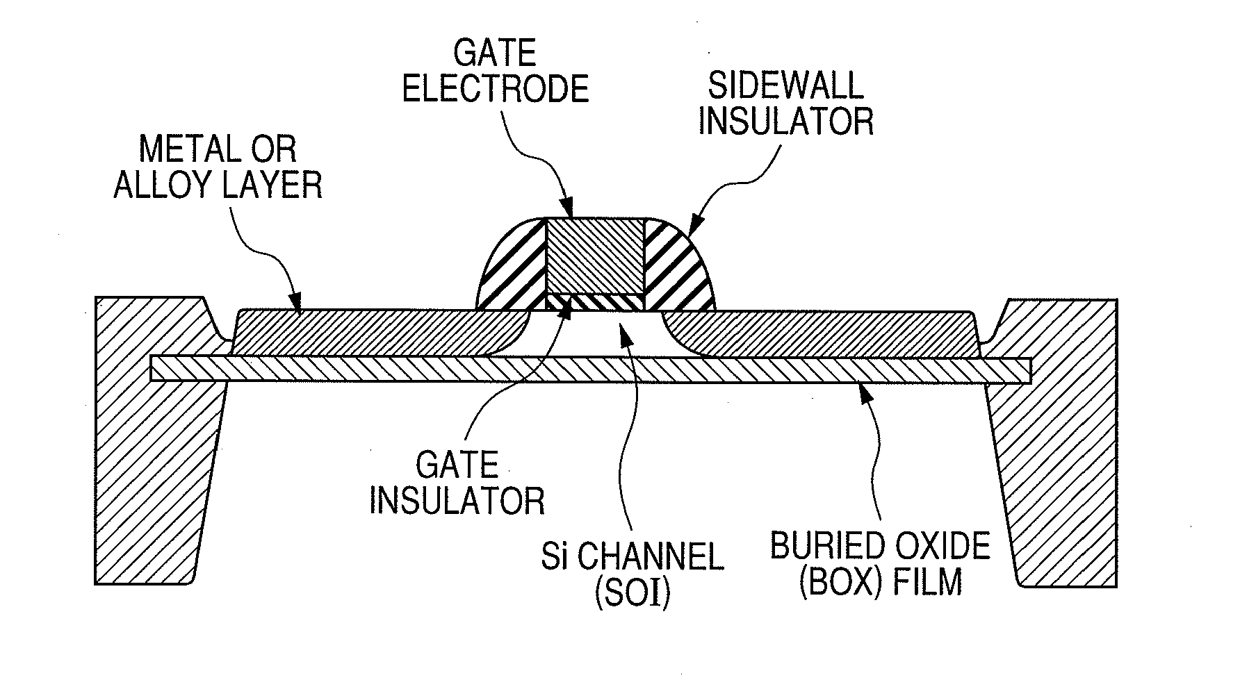
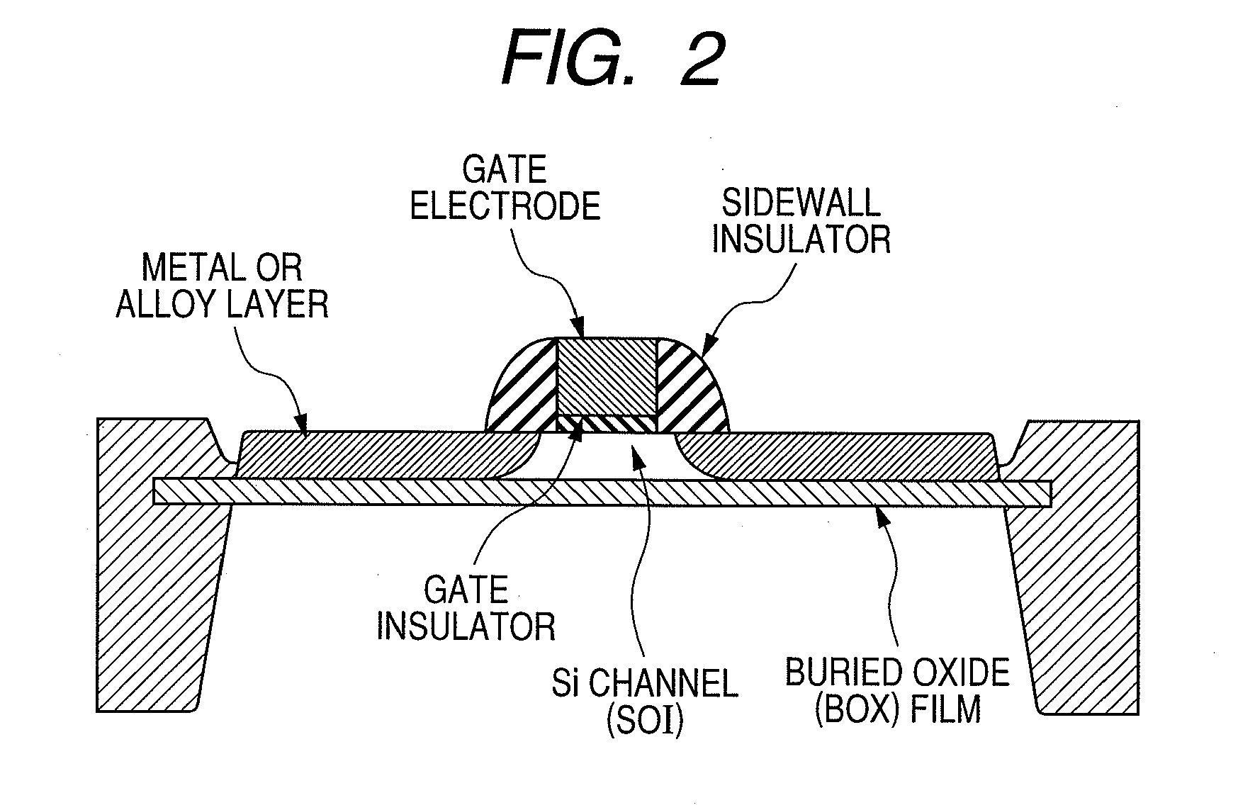
[0053]First, a semiconductor device including a MIS transistor according to a first embodiment of the present invention will be described.

[0054]A method for manufacturing the semiconductor device according to this embodiment is explained in chronological order referring to FIGS. 7 to 15. For simple illustration, only an n-type MIS transistor will be illustrated and described while illustrations and descriptions of the other devices are omitted.

[0055]First, an SOI substrate which includes a supporting substrate 1, a buried insulating layer (BOX layer) 2, and a semiconductor layer (SOI layer) 3 as shown in FIG. 7 is prepared. The supporting substrate 1 is made of p-type monocrystalline silicon having a plane orientation of (100) and a resistivity of about 5 Ωcm. The SOI layer 3 is made of p-type monocrystalline silicon having a plane orientation of (100) and a crystal orientation of in the direction parallel to an orientation flat or notch, and a thickness of 30 nm. The BOX laye...

second embodiment

[0065

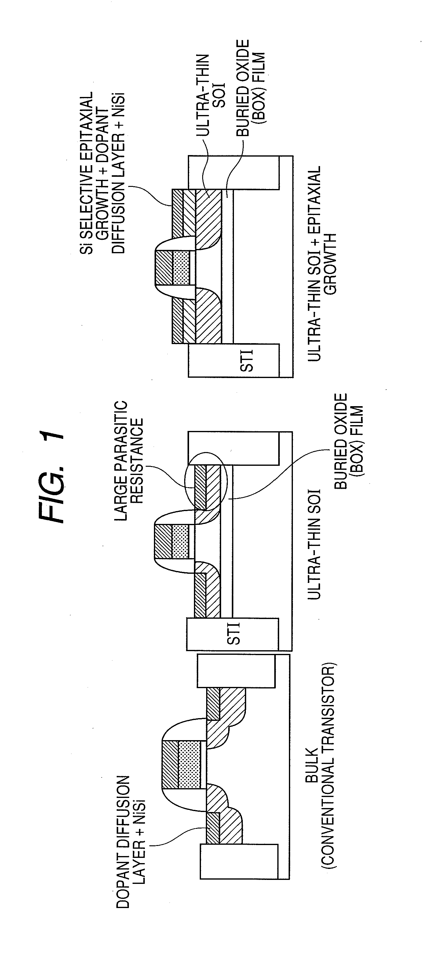
[0066]In the second embodiment, a known photolithographic technique is used to form a p-channel MISFET and complete a CMISFET where the polarities (n type, p type) are reversed in all ion implantation steps. FIG. 17 illustrates the effect of an dopant segregation layer in a semiconductor device according to the second embodiment of the present invention. A p+ / n−abrupt junction is formed by a high-concentration dopant segregation layer; the depletion layer is narrow; and hole injection by tunneling current at the valence band edge increases. In other words, this suggests that the Schottky barrier lowers.

[0067]In this embodiment, by controlling the polycrystalline silicon film thickness, the polycrystalline silicon film can also be fully silicidized to form a full silicide gate electrode. Also a gate electrode may be formed from a metal material such as TiN film using a known gate damascene technique or similar technique. It is needless to say that any other metal may be used to ...


PUM


Abstract

A semiconductor device which includes: a semiconductor layer formed over an insulating layer over a semiconductor substrate; a gate electrode disposed over the semiconductor layer through a gate insulator; a sidewall insulator formed along the gate insulating film and a sidewall of the gate electrode; a source/drain layer including an alloy layer whose bottom surface is in contact with the insulating layer; and an impurity-doped layer which is segregated in a self-aligned manner in an interface between the alloy layer and the semiconductor layer and has a face for junction with a channel region formed along a crystal orientation plane of the semiconductor layer.

Description

CLAIM OF PRIORITY[0001]The present application claims priority from Japanese patent application JP 2009-159412 filed on Jul. 6, 2009, the content of which is hereby incorporated by reference into this application.FIELD OF THE INVENTION[0002]The present invention relates to semiconductor devices and a method for manufacturing the same and more particularly to technology which is useful for a MIS (Metal Insulator Semiconductor) transistor formed on an SOI wafer.BACKGROUND OF THE INVENTION[0003]As for large-scale integrated circuits (LSIs) used in microcomputers for digital appliances and personal computers, there has been demand for higher speed, lower power consumption, and multifunctionality. In electronic devices as circuit components, for example, MIS transistors as typified by silicon (Si) field-effect transistors (FETs), device performance improvements (increase in current driving force and reduction in power consumption) have been so far achieved mainly by shortening the gate l...

Claims


Application Information

Patent Timeline
IPC IPC(8): H01L29/786H01L21/84
CPCH01L21/268H01L21/84H01L29/78618H01L29/41733H01L29/458H01L27/1203
Inventor SHIMA, AKIOSUGII, NOBUYUKI
Owner HITACHI LTD
Why Eureka
Try Eureka