Semiconductor device manufacturing method

a technology of semiconductor devices and manufacturing methods, applied in semiconductor devices, capacitors, electrical equipment, etc., can solve the problems of deterioration of mos transistor characteristics and relative high voltage requirements, and achieve the effects of reducing the resistance of the source/drain region, and increasing the resistance of the refractory metal silicide layer

Active Publication Date: 2006-12-14
FUJITSU SEMICON LTD
View PDF3 Cites 0 Cited by
  • Summary
  • Abstract
  • Description
  • Claims
  • Application Information

AI Technical Summary

Benefits of technology

[0018] According to the present invention, since the annealing is performed for an annealing time such that a agglomeration area of the refractory metal silicide layer becomes equal to or less than an upper limit area, it can be prevented that the resistance of the refractory metal silicide layer is increased due to an increase of the agglomeration area at the annealing. Therefore, even in the case where the refractory metal silicide layer is formed on the source / drain region of the MOS transistor and then the annealing is carried out to the resultant structure, the resistance of the source / drain region can be reduced sufficiently by the refractory metal silicide layer.
[0019] Such annealing includes the recovery annealing for the capacitor dielectric film using the furnace, and the crystallizing annealing conducted by applying the rapid thermal annealing to the ferroelectric film, for example. These annealings are peculiar to the FeRAM, and the large heat load is applied to the refractory metal silicide layer. Therefore, when the annealing time is decided by defining an upper limit area of the agglomeration area as described above, it can be prevented that the resistance of the refractory metal silicide layer is increased.

Problems solved by technology

However, such flash memory possesses a defect that, since a tunnel current must be supplied to the gate insulating film in writing or erasing the information, a relatively high voltage is required.
However, portions other than the capacitor, e.g., a refractory metal sicilide layer on the source / drain region of a MOS transistor, suffers from an unnecessary heat load by these annealings, and hence there arises concern that the characteristics of the MOS transistor are deteriorated.

Method used


Image

  • Semiconductor device manufacturing method
  • Semiconductor device manufacturing method
  • Semiconductor device manufacturing method

Examples


Embodiment Construction

[0032] An embodiment of the present invention will be explained in detail with reference to the accompanying drawings hereinafter.

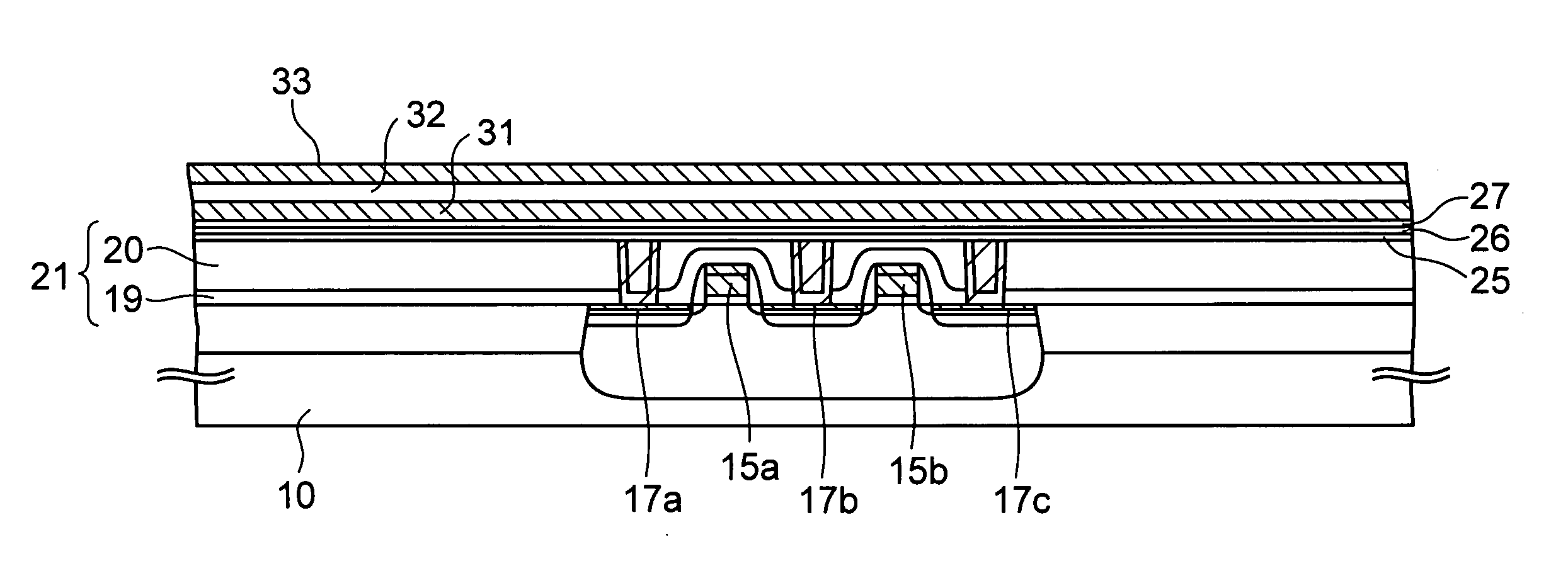
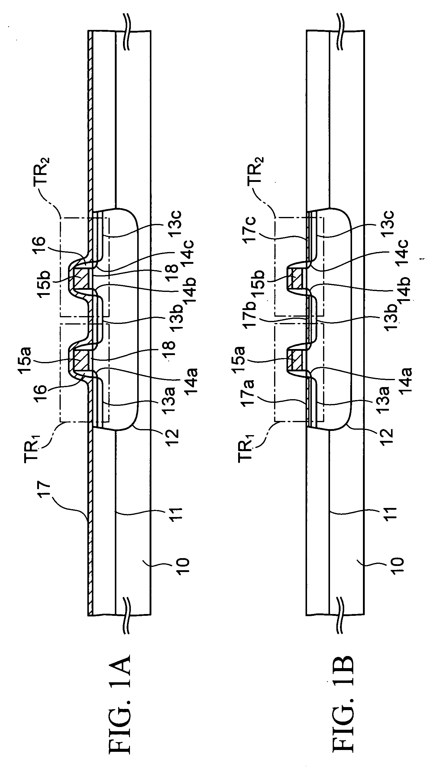
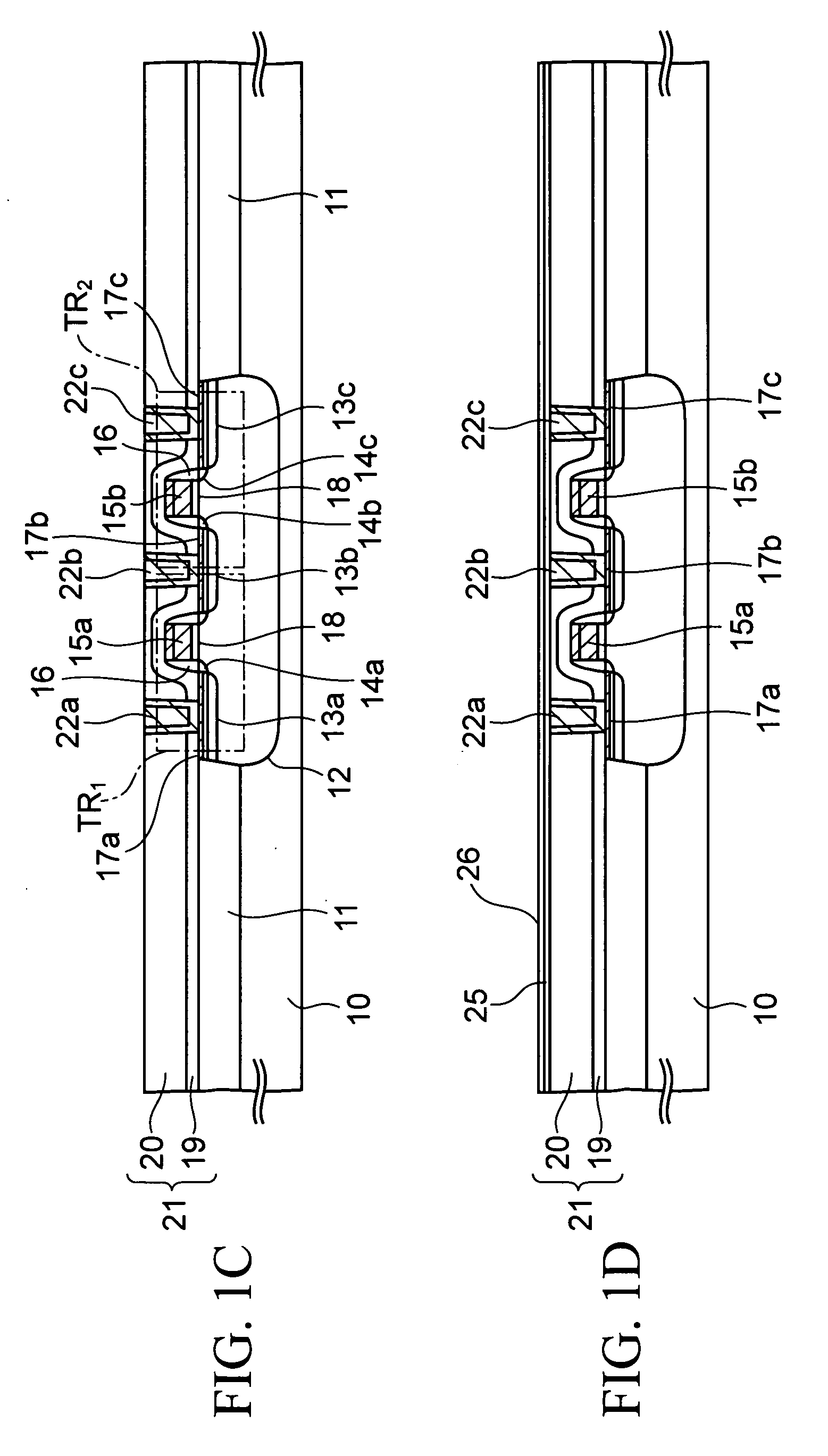
[0033]FIGS. 1A to 1N are sectional views of a semiconductor device according to an embodiment of the present invention in the middle of manufacture.

[0034] First, the steps required until a sectional structure shown in FIG. 1A is obtained will be explained hereunder.

[0035] An STI (Shallow trench Isolation) trench to define an active region of the transistor is formed on a surface of an n-type or p-type silicon (semiconductor) substrate 10. Then, an element isolation insulating film 11 is formed by filling an insulating film such as a silicon oxide film or the like in the trench. Here, an element isolation structure is not limited to STI, and the element isolation insulating film 11 may be formed by the LOCOS (Local Oxidation of Silicon) method.

[0036] Next, a p-well 12 is formed by introducing the p-type impurity into the active region of the silicon su...


PUM

PropertyMeasurementUnit
temperatureaaaaaaaaaa
thicknessaaaaaaaaaa
temperatureaaaaaaaaaa

Abstract

A semiconductor device manufacturing method, includes a step of forming refractory metal silicide layers 13a to 13c in a partial area of a semiconductor substrate 10, a step of forming an interlayer insulating film 21 on the refractory metal silicide layers 13a to 13c, a step of forming a first conductive film 31, a ferroelectric film 32, and a second conductive film 33 in sequence on the interlayer insulating film 21, a step of forming a capacitor Q consisting of a lower electrode 31a, a capacitor dielectric film 32a, and an upper electrode 33a by patterning the first conductive film 33, the ferroelectric film 32, and the second conductive film 31, and a step of performing an annealing for an annealing time to suppress a agglomeration area of the refractory metal silicide layers 13a to 13c within an upper limit area.

Description

CROSS-REFERENCE TO RELATED APPLICATIONS [0001] This application is based on and claims priority of Japanese Patent Application No. 2005-168603 filed on Jun. 8, 2005, the entire contents of which are incorporated herein by reference. BACKGROUND OF THE INVENTION [0002] 1. Field of the Invention [0003] The present invention relates to a semiconductor device manufacturing method. [0004] 2. Description of the Related Art [0005] As the nonvolatile memory that can store information after a power supply is turned off, the flash memory and the ferroelectric memory are known. [0006] Out of them, the flash memory has a floating gate that is buried in a gate insulating film of an insulated-gate field effect transistor (IGFET), and stores information by accumulating a charge representing the stored information in this floating gate. However, such flash memory possesses a defect that, since a tunnel current must be supplied to the gate insulating film in writing or erasing the information, a rela...

Claims


Application Information

Patent Timeline
Patent Type & Authority Applications(United States)
IPC IPC(8): H01L21/8244
CPCH01L21/28518H01L28/55H01L27/11507H01L27/11502H10B53/30H10B53/00
Inventor HIKOSAKA, YUKINOBUTACHIBANA, HIROTOSHI
Owner FUJITSU SEMICON LTD
Why Eureka
Try Eureka