Substrate assembly for crystal growth and fabricating method for light emitting device using the same

Inactive Publication Date: 2013-01-31
SEOUL VIOSYS CO LTD
View PDF3 Cites 2 Cited by
  • Summary
  • Abstract
  • Description
  • Claims
  • Application Information

AI Technical Summary

Benefits of technology

[0024]According to the present invention, there is provided a substrate assembly for crystal growth and a fabricating method of a light emitting device using the same, which, even though the size and thickness of a substrate for growing the light emitti

Problems solved by technology

As the size and thickness of the substrate is increased, the time and the cost spent for the process are increased.
For example, th

Method used


Image

  • Substrate assembly for crystal growth and fabricating method for light emitting device using the same
  • Substrate assembly for crystal growth and fabricating method for light emitting device using the same
  • Substrate assembly for crystal growth and fabricating method for light emitting device using the same

Examples


Embodiment Construction

[0030]Hereinafter, preferred embodiments of the present invention will be described in detail with reference to the accompanying drawings. The following embodiments are provided only for illustrative purposes so that those skilled in the art can fully understand the spirit of the present invention. Therefore, the present invention is not limited to the following embodiments but may be implemented in other forms. In the drawings, the widths, lengths, thicknesses and the like of elements are exaggerated for convenience of illustration. Like reference numerals indicate like elements throughout the specification and drawings.

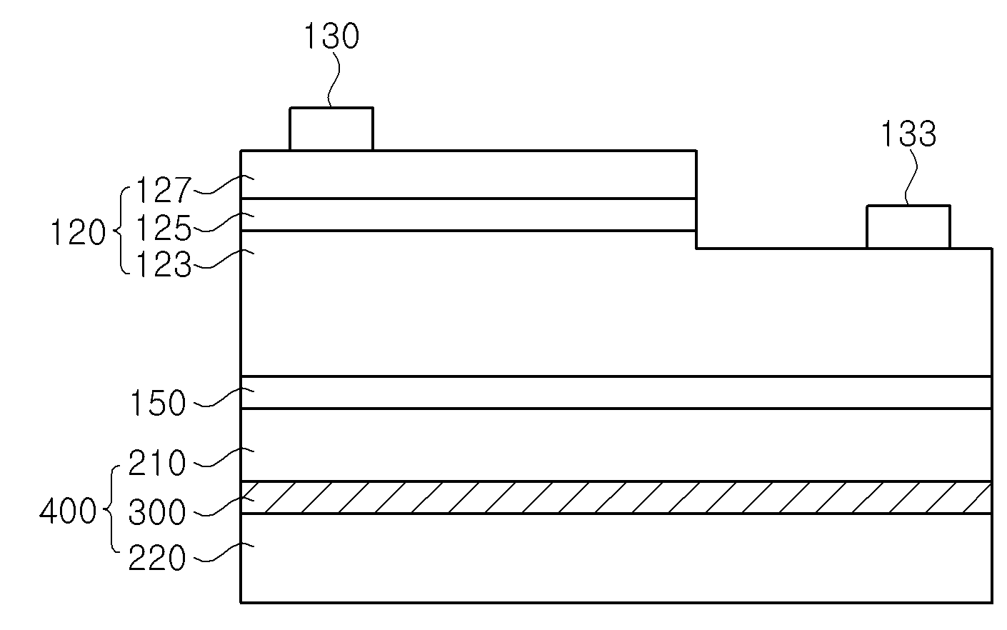
[0031]FIG. 1 is a sectional view illustrating a substrate assembly according to an embodiment of the present invention.

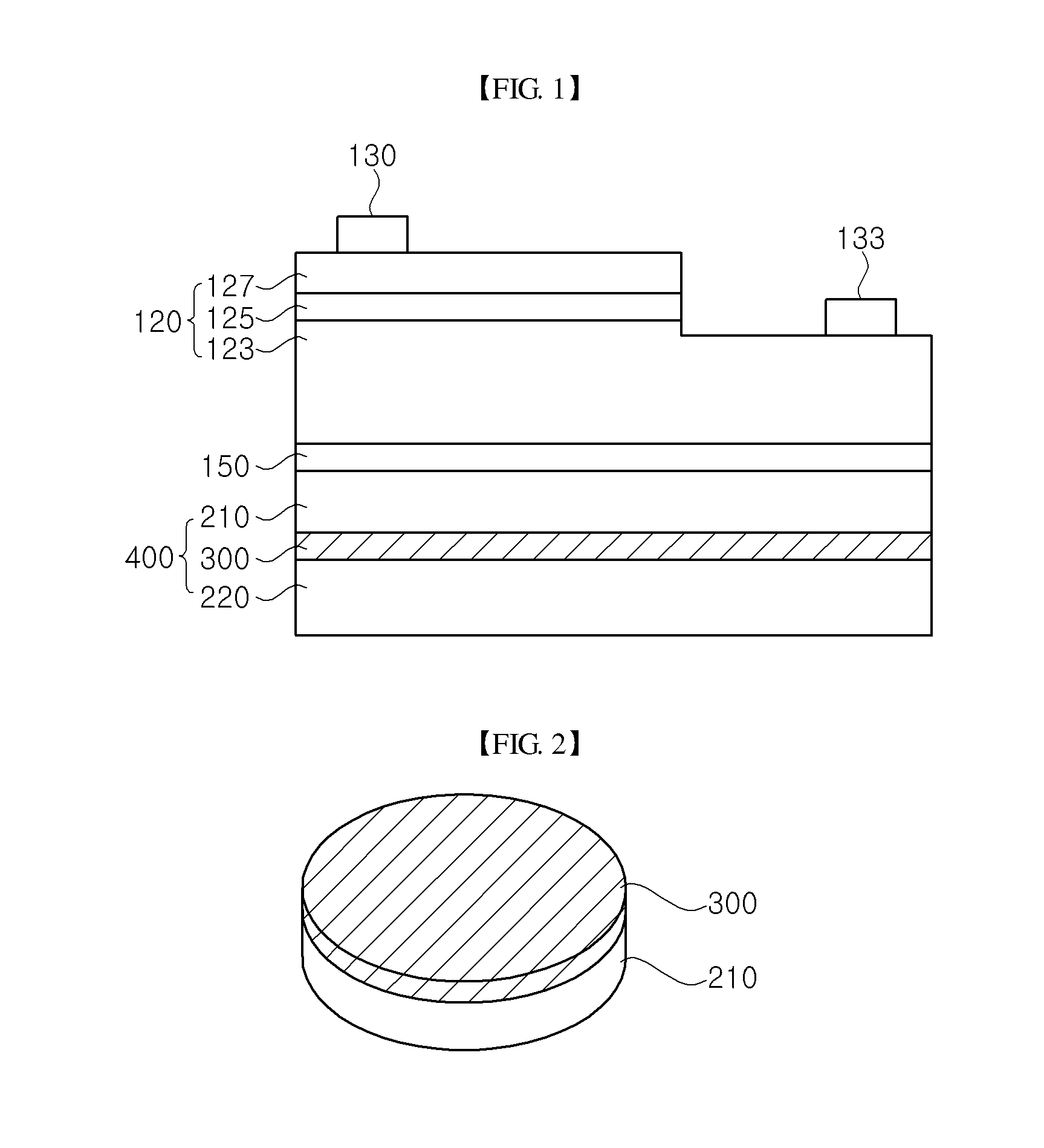
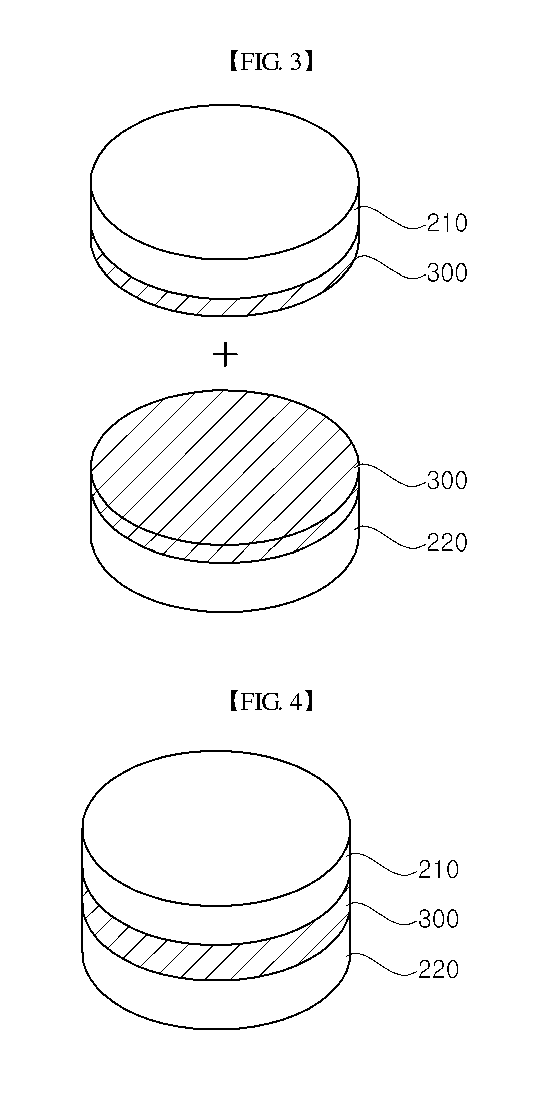
[0032]Referring to FIG. 1, the substrate assembly 400 according to the embodiment of the present invention includes a first substrate 210, a second substrate 220 and a bonding layer 300. A semiconductor lamination structure 120 including an N-type s...


PUM

PropertyMeasurementUnit
Semiconductor propertiesaaaaaaaaaa
Thermal expansion coefficientaaaaaaaaaa

Abstract

A substrate assembly on which a first conduction-type semiconductor layer, an active layer and a second conduction-type semiconductor layer are formed is disclosed, the substrate assembly comprising a first substrate, a second substrate and a bonding layer interposed there between. In the substrate assembly, the thermal expansion coefficient of the bonding layer is smaller than or equal to that of at least one of the first and second substrates.

Description

CROSS-REFERENCE TO RELATED APPLICATIONS[0001]This application is the National Stage of International Application PCT / KR2011 / 002454, filed on Apr. 7, 2011, and claims priority from and the benefit of Korean Patent Application No. 10-2010-0033113, filed on Apr. 12, 2010, both of which are incorporated herein by reference for all purposes as if fully set forth herein.BACKGROUND[0002]1. Field[0003]The present invention relates to a substrate assembly for crystal growth and a fabricating method of a light emitting device using the same. More particularly, the present invention relates to a substrate assembly for crystal growth including a bonding layer and a is fabricating method of a light emitting device using the substrate assembly.[0004]2. Discussion of the Background[0005]In general, since Group-III-element nitrides, such as GaN and AlN, have an excellent thermal stability and a direct-transition-type energy band structure, the Group-III-element nitrides have recently come into the ...

Claims


Application Information

Patent Timeline
IPC IPC(8): H01L33/48B32B9/04B32B7/02B32B15/04
CPCY10T428/24942H01L33/0079H01L33/0093
Inventor LEE, CHUNG HOONYE, KYUNG HEEKAL, DAE SUNGSEO, WON CHEOL
Owner SEOUL VIOSYS CO LTD
Why Eureka
Try Eureka