Monolithic ceramic electronic component

a technology of monolithic ceramic and electronic components, applied in the direction of fixed capacitor details, generators/motors, fixed capacitors, etc., can solve the problems of difficult forming of outer electrodes with high accuracy, limited accuracy of applying thick film paste, and general degradation of monolithic ceramic electronic components, so as to reduce the local shortening distance between the inner electrodes, prevent degradation of reliability, and facilitate the effect of forming outer electrodes

Active Publication Date: 2013-02-07
MURATA MFG CO LTD
View PDF3 Cites 35 Cited by
  • Summary
  • Abstract
  • Description
  • Claims
  • Application Information

AI Technical Summary

Benefits of technology

[0013]Accordingly, preferred embodiments of the present invention provide a monolithic ceramic electronic component having a structure that can solve the problem mentioned above.
[0021]Further, the inventors have discovered that such a sinking phenomenon is apt to more easily occur in particular when the first lead-out portion is led out from the longer side of the first opposing portion.
[0022]With the preferred embodiments of the present invention, in the monolithic ceramic electronic component including the inner electrodes each of which has the first lead-out portion led out from the longer side of the first opposing portion, a density of the outer-layer dummy conductors in the outer layer portion is reduced. Therefore, the pressing of the inner electrodes through the outer-layer dummy conductors is relieved in the pressing step before firing such that the distance between the inner electrodes can be prevented from being locally shortened. It is hence possible to effectively reduce and prevent degradation of reliability of the monolithic ceramic electronic component, e.g., a reduction of BDV, which may be caused by the local shortening of the distance between the inner electrodes.
[0023]In relation to the preferred embodiments of the present invention, from the viewpoint of reducing and preventing the degradation of reliability, the interval d1 between the outer-layer dummy conductors adjacent to each other is preferably longer. However, the longer the interval d1, the stronger a tendency to impede growth of the plated film for the first outer electrode. Stated another way, a risk that plated films growing with the exposed portions of the outer-layer dummy conductors being nuclei may become hard to continuously join with each other in the height direction is increased. For that reason, the interval d1 is preferably set so as to satisfy d1≦about 6 μm. By satisfying that condition, the growth of the plated film for the first outer electrode can be more reliably ensured.

Problems solved by technology

As a result, characteristics of the monolithic ceramic electronic component generally tend to degrade.
However, a known method of baking a thick film paste has a limit in accuracy of applying the paste and has a difficulty in forming the outer electrodes with high accuracy.
With the method disclosed in Japanese Unexamined Patent Application Publication No. 2004-327983, however, reliability, e.g., BDV (breakdown voltage), of the monolithic ceramic electronic component may degrade in some cases.
As a result, it has been discovered that the degradation of reliability (BDV) is attributable to the presence of the dummy conductors.

Method used


Image

  • Monolithic ceramic electronic component
  • Monolithic ceramic electronic component
  • Monolithic ceramic electronic component

Examples


first preferred embodiment

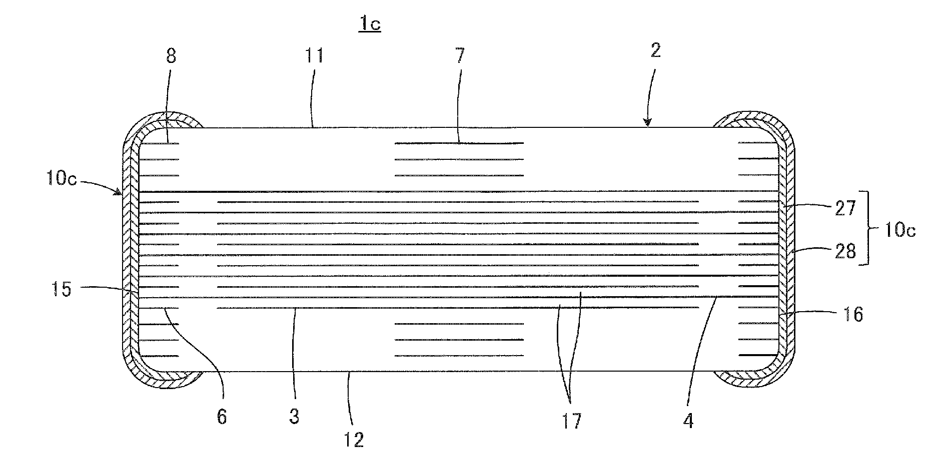
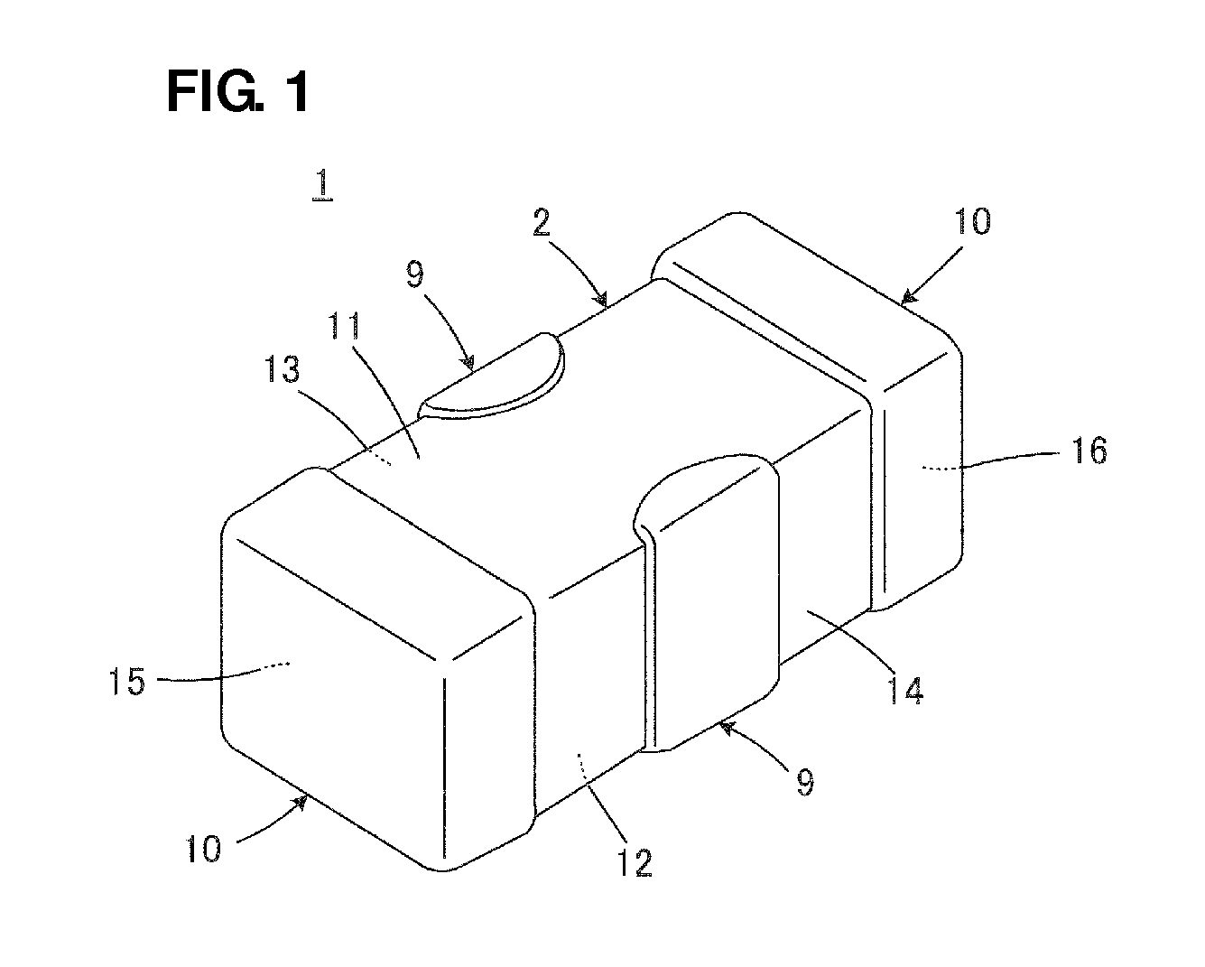
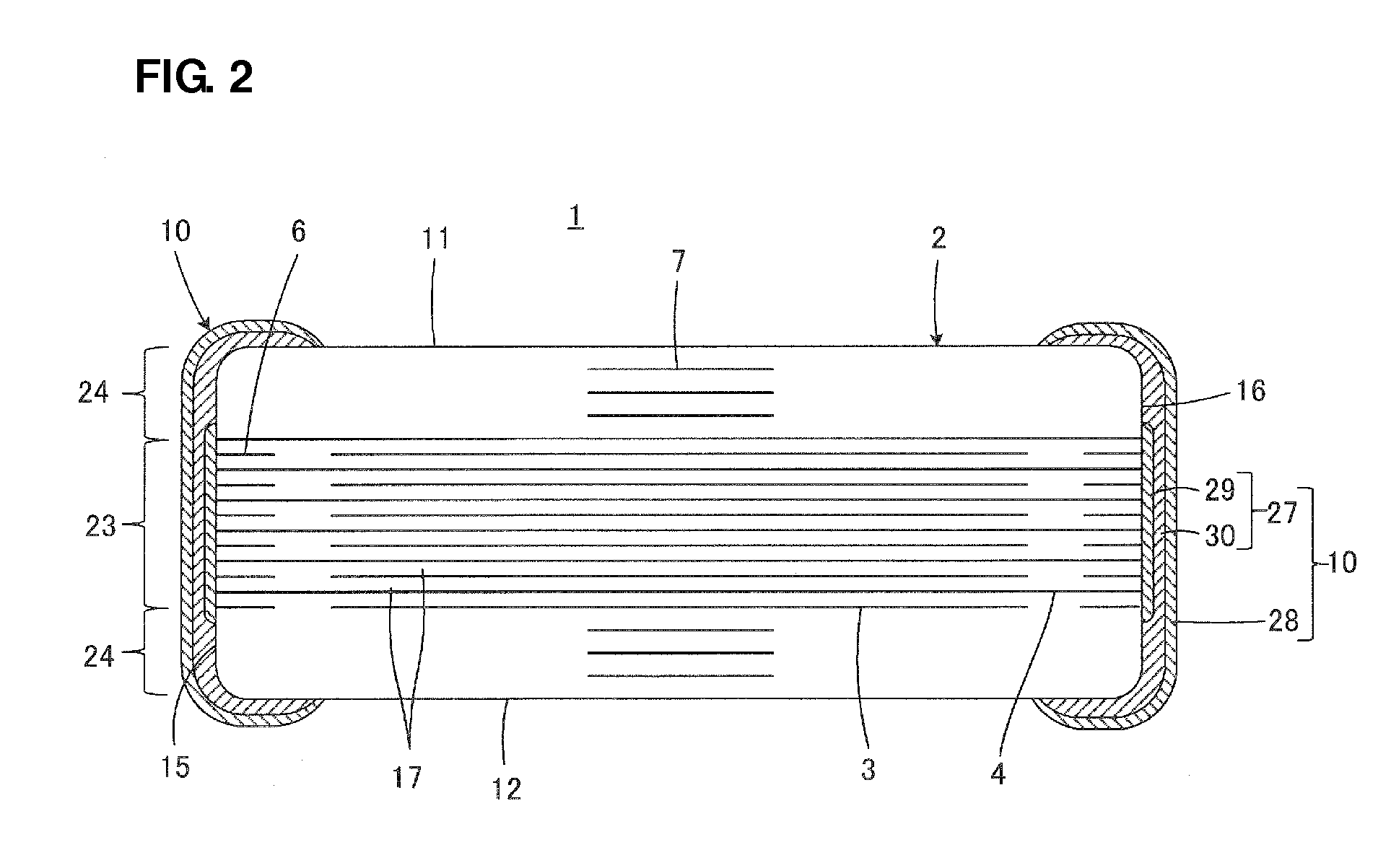
[0038]A first preferred embodiment of the present invention will be described below with reference to FIGS. 1 to 7. A monolithic ceramic capacitor 1 according to the first preferred embodiment includes a ceramic base element 2. The monolithic ceramic capacitor 1 further includes first and second inner electrodes 3 and 4, first and second inner-layer dummy conductors 5 and 6, and outer-layer dummy conductors 7, which are all disposed inside the ceramic base element 2, as well as first and second outer electrodes 9 and 10, which are disposed on outer surfaces of the ceramic base element 2. Details of the structure of the monolithic ceramic capacitor 1 will be described below followed by a description of a manufacturing method.

[0039]The ceramic base element 2 preferably is substantially parallelepiped, and includes outer surfaces defined by a pair of first and second principal surfaces 11 and 12 opposed to each other, a pair of lateral surfaces 13 and 14 opposed to each other, and a pa...

second preferred embodiment

[0100]A second preferred embodiment of the present invention is illustrated in FIG. 8. FIG. 8 is a sectional view corresponding to FIG. 3. Equivalent elements in FIG. 8 to those in FIG. 3 are denoted by the same reference symbols and duplicate descriptions of those elements are omitted here.

[0101]In a monolithic ceramic capacitor 1a according to the second preferred embodiment, an outer-layer dummy conductor 7a is arranged such that the outer-layer dummy conductor 7a does not penetrate through the ceramic base element 2 in the widthwise direction and it is separated in the widthwise direction.

third preferred embodiment

[0102]A third preferred embodiment of the present invention is illustrated in FIGS. 9 and 10. FIG. 9 is a perspective view corresponding to FIG. 1, and FIG. 10 is a sectional view corresponding to FIG. 3. Equivalent elements in FIGS. 9 and 10 to those in FIGS. 1 and 3 are denoted by the same reference symbols and duplicate descriptions of those elements are omitted here.

[0103]A monolithic ceramic capacitor 1b according to the third preferred embodiment is characterized in that a first outer electrode 9b, including an underlying layer 25 and an overlying layer 26 thereof, is disposed to extend over the first and second lateral surfaces 13 and 14 and the first and second principal surfaces 11 and 12 of the ceramic base element 2 in a fully surrounding state.

[0104]In this preferred embodiment, the outer-layer dummy conductors 7 are preferably exposed in at least respective portions of the principal surfaces 11 and 12 by chipping off the ceramic layers 17, which define the principal sur...


PUM

PropertyMeasurementUnit
thicknessaaaaaaaaaa
thicknessaaaaaaaaaa
thicknessaaaaaaaaaa

Abstract

In a monolithic ceramic electronic component, given that an interval between outer-layer dummy conductors adjacent to each other in an outer layer portion is d1, and that an interval between first and second inner electrodes adjacent to each other in an inner layer portion is d2, 1.7d2≦d1 is satisfied. By reducing a density of the outer-layer dummy conductors in the outer layer portion on that condition, pressing of the inner electrodes through the outer-layer dummy conductors is relieved in a pressing step before firing. As a result, a distance between the inner electrodes can be prevented from being locally shortened. It is hence possible to effectively reduce and prevent degradation of reliability of the monolithic ceramic electronic component, e.g., a reduction of BDV.

Description

BACKGROUND OF THE INVENTION[0001]1. Field of the Invention[0002]The present invention relates to a monolithic ceramic electronic component, and more particularly to a monolithic ceramic electronic component provided with outer electrodes including plated films that are disposed and formed directly on outer surfaces of a ceramic base element.[0003]2. Description of the Related Art[0004]Recently, the sizes of electronic devices, such as cellular phones, notebook personal computers, digital cameras, and digital audio devices, have been reduced more and more. Monolithic ceramic electronic components capable of being manufactured with smaller sizes and higher performance have been used in many of these electronic devices.[0005]The monolithic ceramic electronic component usually includes a ceramic base element including a plurality of stacked ceramic layers, inner electrodes formed inside the ceramic base element, and outer electrodes formed on outer surfaces of the ceramic base element. ...

Claims


Application Information

Patent Timeline
Patent Type & Authority Applications(United States)
IPC IPC(8): H01G4/30H01C7/13H01L41/047
CPCH01G4/30H01G4/232H01L41/0471H01G4/012H01C1/148H01C7/18H01G4/005H10N30/871H01G4/12
Inventor SAKURATANI, MASAHIROAKAZAWA, TEPPEI
Owner MURATA MFG CO LTD
Why Eureka
Try Eureka