Light emitting device and method for manufacturing the same

a technology of light emitting devices and manufacturing methods, which is applied in the manufacture of electrode systems, electric discharge tubes/lamps, and discharge tubes luminescnet screens, etc., can solve the problems of light decay, limited surface, and the minimum cavity size of the cup or recess that can be processed, so as to reduce the size, reduce the effect of light extraction efficiency and suppress the degradation of optical characteristics

Active Publication Date: 2013-02-07
STANLEY ELECTRIC CO LTD
View PDF1 Cites 37 Cited by
  • Summary
  • Abstract
  • Description
  • Claims
  • Application Information

AI Technical Summary

Benefits of technology

[0014]According to the presently disclosed subject matter, light emitted from the side of the light emitting element is not returned to the inside of the light emitting element, but can be reflected by a slope of a reflection material layer, and therefore the light ext...

Problems solved by technology

However, the minimum size of the cavity such as cup or recess that can be processed to have a desired shape of internal surface is limited, and the size of the opening (light emitting surface) is necessarily becomes larger than the upper surface of the light emitting element.
There is also a problem that, since the light penetrates through the flu...

Method used


Image

  • Light emitting device and method for manufacturing the same
  • Light emitting device and method for manufacturing the same
  • Light emitting device and method for manufacturing the same

Examples


example 1

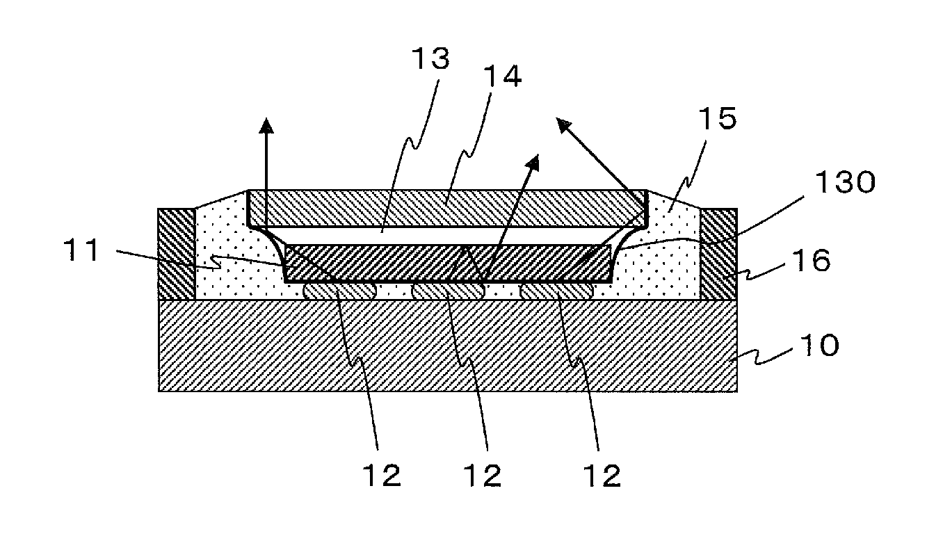
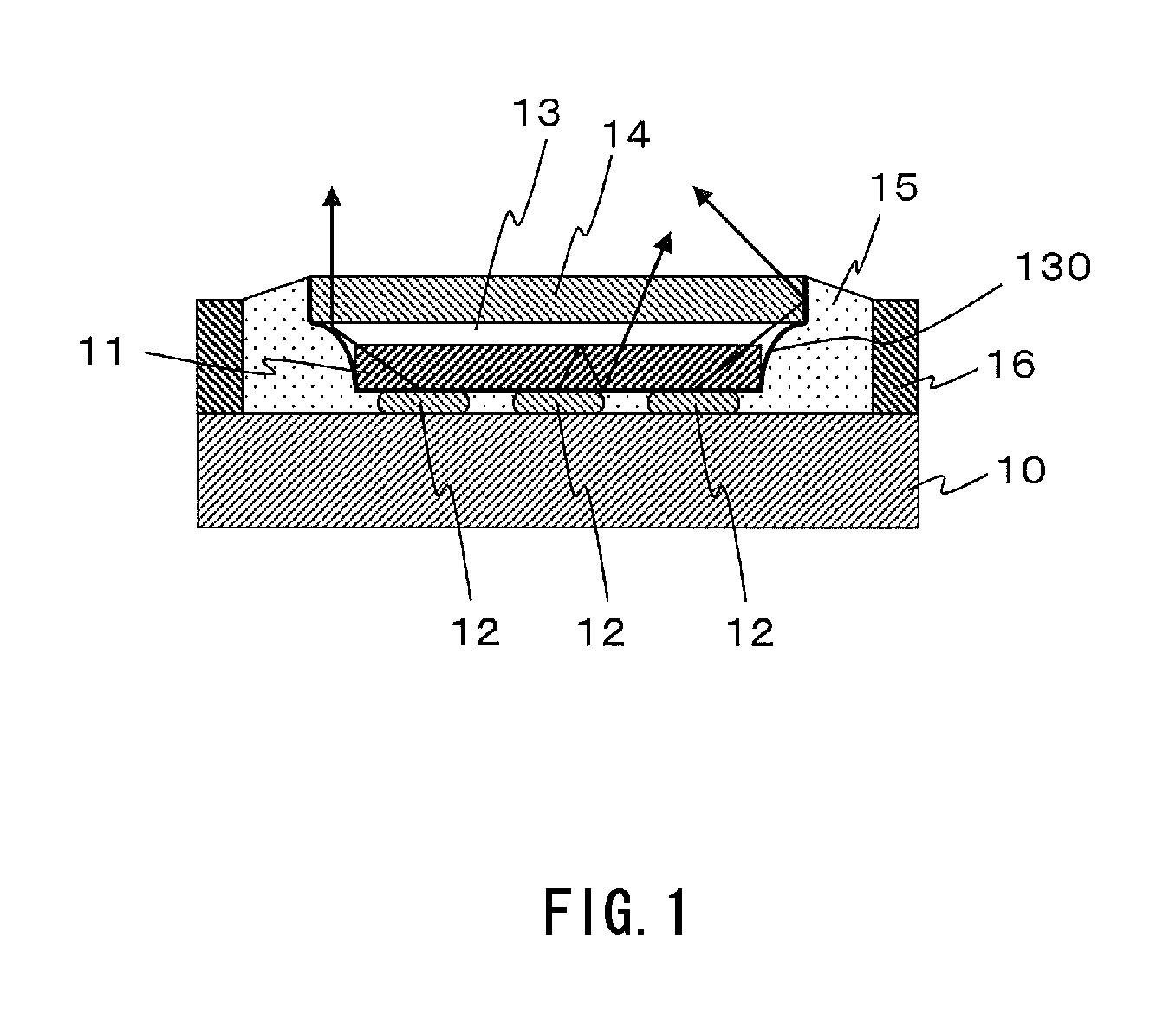
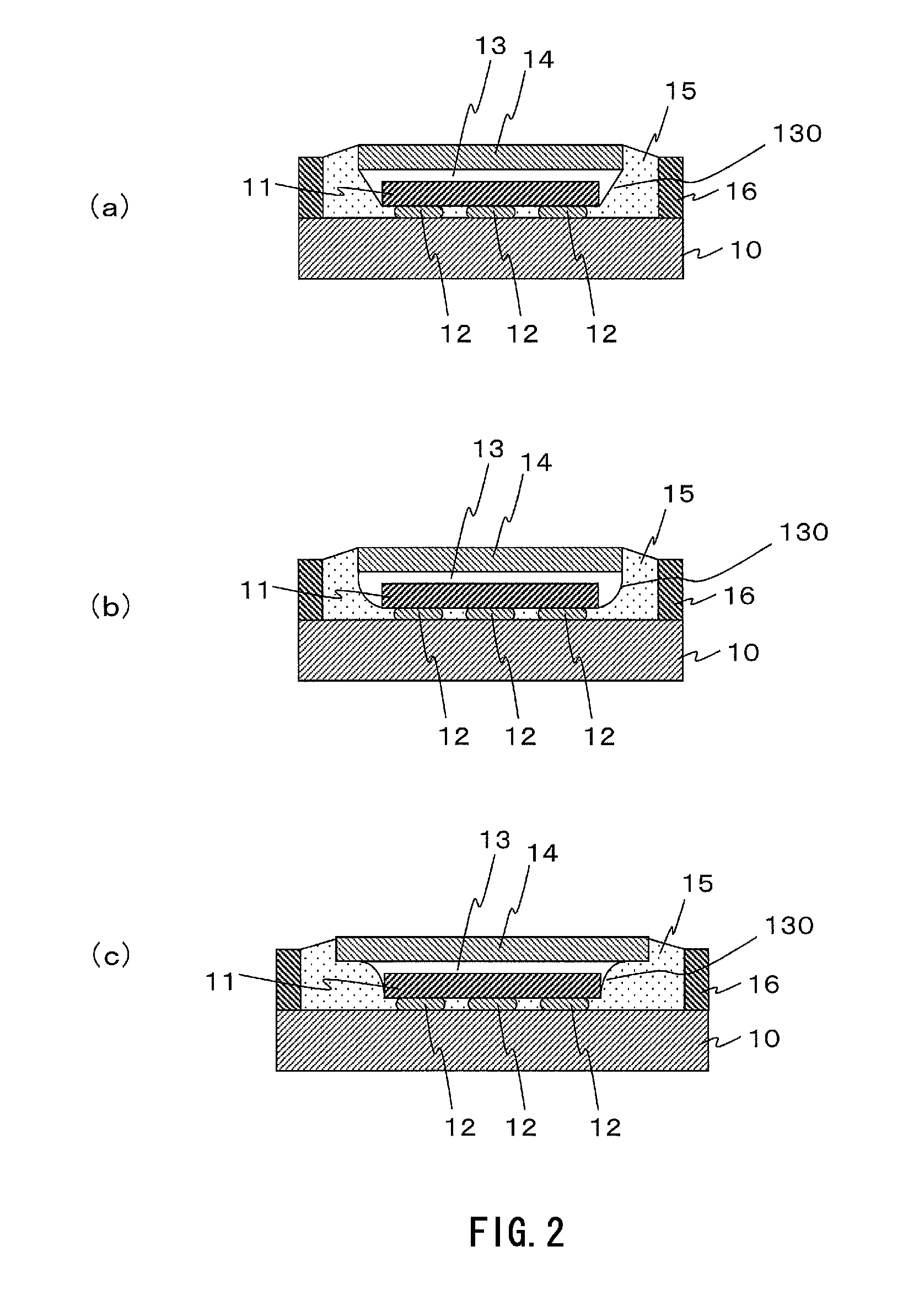
[0122]As Example 1, a light emitting device having the structure shown in FIG. 12 was produced. There was prepared a submount substrate 10 on which a flip chip type light emitting element 11 in the shape of a 1-mm square having a thickness of 100 μm was mounted. To a silicone resin, 60% by weight of a YAG fluorescent substance having a particle size of 15 μm as the fluorescent substance particles 13a, and 5% by weight of silica glass spherical beads (mean particle size: 40±4 μm, CV value: ±3.5%, purity of SiO2: 99.9%, produced by Ube-Nitto Kasei Co., Ltd.) as the spacer 13b were added, and they were sufficiently kneaded to attain uniform dispersion and thereby obtain a paste 13′.

[0123]About 7.0×10⁻⁴ ml of the above paste 13′ was applied on the upper surface of the light emitting element 11 as the paste 13′. A tabular member 14 of alkali-free glass in the shape of a 1.2 mm-square having a thickness of 0.1 mm (alkali metal oxide content: not higher than 0.1% by weight, OA-10G, produce...

example 2

[0125]As Example 2, a light emitting device was produced in the same manner as that used in Example 1, except that the spacer 13b was changed to spherical beads consisting of titanium barium glass (median particle size: 41±2 μm, particle size variation: ±3 μm, alkali metal oxide content: lower than 0.2% by weight, containing TiO2, ZnO, BaG, ZrO2, CaO, and SiO2, GS40S, Nippon Electric Glass Co., Ltd.), and the material of the tabular member 14 was changed to alkali-free glass (alkali metal oxide content: not higher than 0.2% by weight, AF45, produced by SCHOTT Nippon K.K.).

example 3

[0126]As Example 3, a light emitting device was produced in the same manner as that used in Example 1, except that the spacer 13b was changed to spherical beads consisting of titanium barium glass (median particle size: 41±2 μm, particle size variation: ±3 μm, alkali metal oxide content: lower than 0.2% by weight, containing TiO2, ZnO, BaG, ZrO2, CaO, and SiO2, GS40S, Nippon Electric Glass Co., Ltd.).


PUM


Abstract

There is provided a method for producing a light emitting device having a small light emitting area and showing high light extraction efficiency. An uncured resin 13′ is dropped on either one or both of a light emitting element 11 and a tabular member 14 in such an amount that the resin is maintained on them by surface tension, the light emitting element 11 and the tabular member 14 are piled up with the uncured resin 13′ maintained between them and on a side of the light emitting element by surface tension of the uncured resin 13′ to form an uncured resin layer 13′ having an inclined side 130, and then the resin layer 13 is cured. The tabular member is constituted with a material having an alkali metal oxide content of 0.2% by weight or lower.

Description

[0001]This application claims the priority benefit under 35 U.S.C. §119 of Japanese Patent Application No. 2011-172274 filed on Aug. 5, 2011, which is hereby incorporated in its entirety by reference.TECHNICAL FIELD[0002]The presently disclosed subject matter relates to a light emitting device that converts light from a light emitting element with a wavelength conversion layer, and a method for manufacturing the same.BACKGROUND ART[0003]There are known light emitting devices that convert a part of light from a light emitting element into light of a different wavelength, mix the converted light and the light from the light emitting element and emit the mixed light. As configurations of such light emitting devices using a fluorescent substance-containing layer, there are known structures in which a light emitting element is disposed in a cup, and the cup is filled with a fluorescent substance-containing resin, or only the opening of the cup is covered with a fluorescent substance-cont...

Claims


Application Information

Patent Timeline
IPC IPC(8): H01J1/62H01J9/00
CPCH01L33/505H01L33/54H01L33/56H01L25/0753H01L33/60H01L2224/16225H01L2224/73253H01L2224/92225H01L2924/0002H01L33/48H01L33/52H01L2924/00
Inventor ITO, KOSABUROSEKO, TOSHIHIROUENO, KAZUHIKOSUZUKI, NAOTO
Owner STANLEY ELECTRIC CO LTD
Why Eureka
Try Eureka