Semiconductor structure having a wetting layer

a technology of wetting layer and semiconductor structure, applied in the direction of semiconductor devices, electrical equipment, nanotechnology, etc., can solve the problems of structural and fabrication difficulties of metal gate structures containing aluminum

Active Publication Date: 2013-02-14
GLOBALFOUNDRIES US INC
View PDF1 Cites 23 Cited by
  • Summary
  • Abstract
  • Description
  • Claims
  • Application Information

AI Technical Summary

Benefits of technology

[0006]According to a third aspect of the exemplary embodiments, there is provided a method of forming a semiconductor structure which includes forming a dummy gate on a semiconductor substrate; forming a spacer on the dummy gate structure; removing the dummy gate to form a trench or via; depositing a gate dielectric in the trench or via; depositing a wetting layer selected from the group consisting of cobalt and nickel to line the trench or via, the wetting layer having an oxygen content of no more than about 200 ppm (parts per million) oxygen and formed by cobalt amidinate or nickel amidinate deposited by a chemical vapor deposition process wherein the cobalt amidinate or nickel amidinate has the formula [M(AMD)2], and the structure

Problems solved by technology

The fabrication of metal gate structures containing aluminum present structural and fabrication difficulties because of aluminum's affinity for oxygen.

Method used


Image

  • Semiconductor structure having a wetting layer
  • Semiconductor structure having a wetting layer
  • Semiconductor structure having a wetting layer

Examples


Embodiment Construction

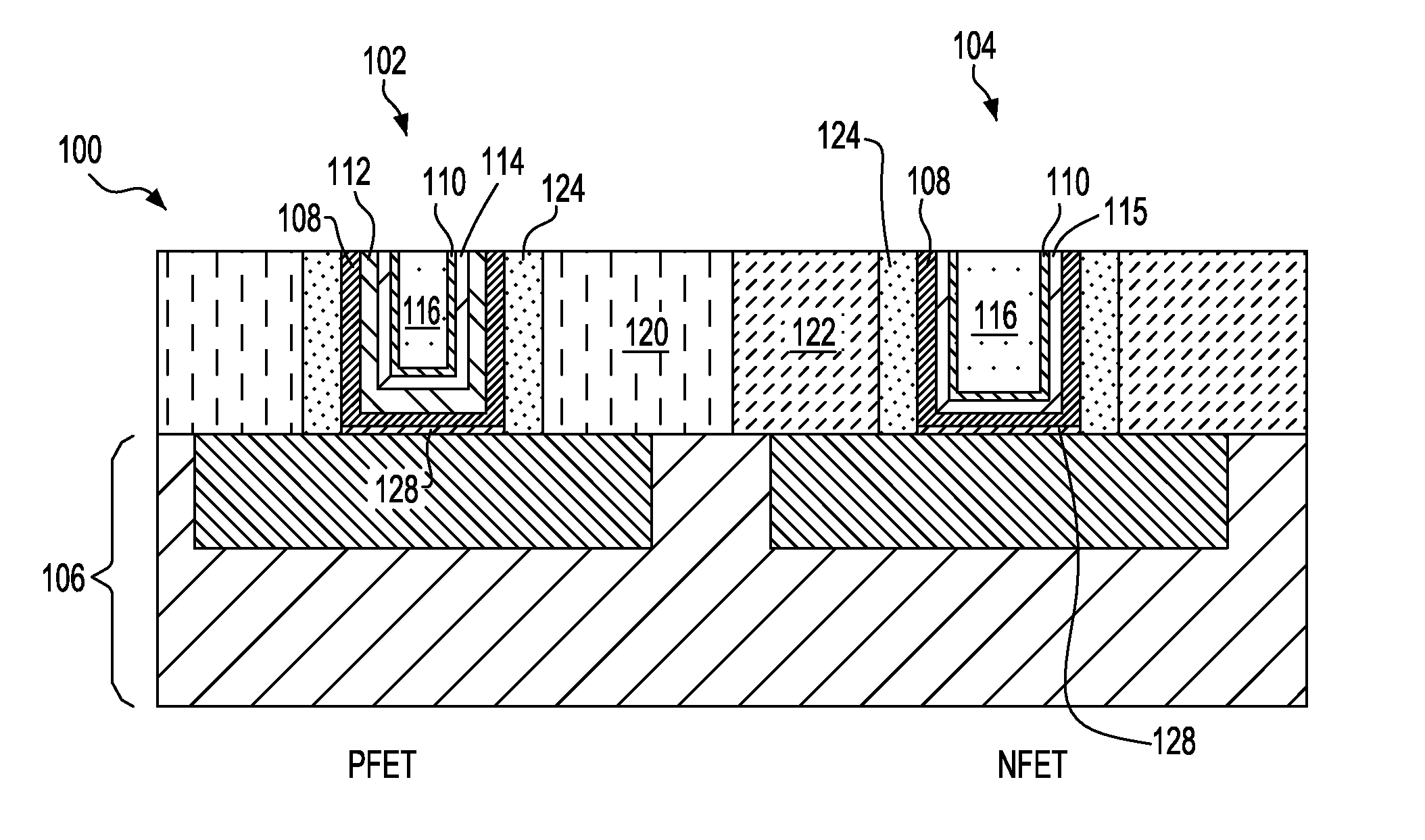
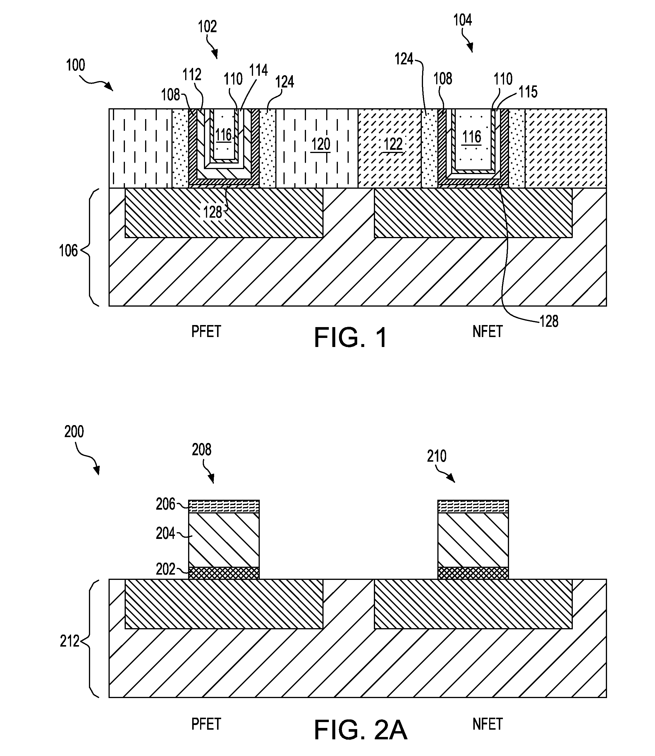
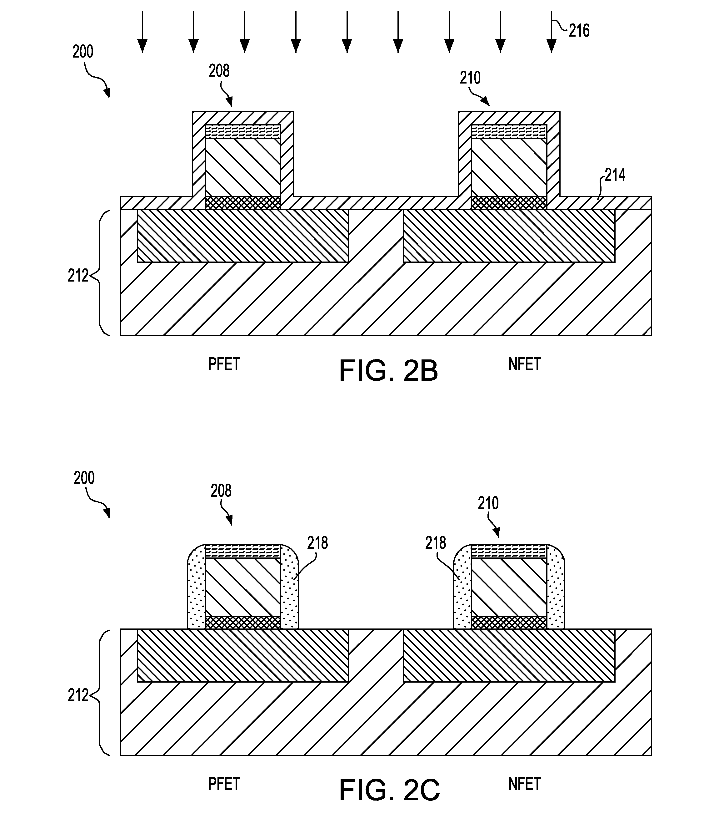
[0023]It is proposed to utilize a chemical vapor deposited (CVD) cobalt or nickel wetting layer in advanced metal gate structures. In a replacement gate device, aluminum is used as the conductor metal because of the low resistivity. Making a void-free aluminum fill for the advanced gate device is very challenging due to the small opening dimension and high aspect ratio of the gate after the work function, barrier and other layers may be deposited. A thin and continuous wetting layer is preferred to be deposited before the aluminum deposition. The wetting layer facilitates the aluminum to reflow into the gate. Aluminum reflow is usually done by keeping the wafer at an elevated temperature during and after the aluminum deposition. Aluminum deposition may be done by a combination of chemical vapor deposition (CVD) and physical vapor deposition (PVD). A desirable wetting layer should have a high affinity with aluminum and should be as thin as possible to allow more room for the aluminum...


PUM

PropertyMeasurementUnit
thicknessaaaaaaaaaa
thicknessaaaaaaaaaa
dielectric constantaaaaaaaaaa

Abstract

A semiconductor structure which includes a semiconductor substrate and a metal gate structure formed in a trench or via on the semiconductor substrate. The metal gate structure includes a gate dielectric; a wetting layer selected from the group consisting of cobalt and nickel on the gate dielectric lining the trench or via and having an oxygen content of no more than about 200 ppm (parts per million) oxygen; and an aluminum layer to fill the remainder of the trench or via. There is also disclosed a method of forming a semiconductor structure in which a wetting layer is formed from cobalt amidinate or nickel amidinate deposited by a chemical vapor deposition process.

Description

BACKGROUND[0001]The present invention relates to semiconductor structures and, more particularly, relates to semiconductor structures which include a cobalt or nickel wetting layer prior to the deposition of an aluminum layer.[0002]Advanced metal gate structures for the 22 nm (nanometer) node and beyond may include an aluminum layer. The fabrication of metal gate structures containing aluminum present structural and fabrication difficulties because of aluminum's affinity for oxygen.[0003]These advanced metal gate structures may be fabricated by a replacement gate process. In a replacement gate process, a polysilicon dummy gate is formed and bracketed with spacers and possibly other materials, the polysilicon dummy gate is removed and then replaced with materials that will form the final gate structure.BRIEF SUMMARY[0004]The various advantages and purposes of the exemplary embodiments as described above and hereafter are achieved by providing, according to a first aspect of the exemp...

Claims


Application Information

Patent Timeline
Patent Type & Authority Applications(United States)
IPC IPC(8): H01L21/28H01L29/78B82Y99/00
CPCH01L21/823842H01L29/66545H01L21/32056H01L21/28079
Inventor NOGAMI, TAKESHIWONG, KEICH KWONG HONYANG, CHIH-CHAO
Owner GLOBALFOUNDRIES US INC
Why Eureka
Try Eureka