Semiconductor Structure with Galvanic Isolation

a technology of a semiconductor structure and a galvanic isolation, applied in the direction of semiconductor/solid-state device details, diodes, capacitors, etc., can solve the problems of a two and a single-dap lead frame that cannot be welded

Active Publication Date: 2013-02-14
NAT SEMICON CORP
View PDF4 Cites 38 Cited by
  • Summary
  • Abstract
  • Description
  • Claims
  • Application Information

AI Technical Summary

Problems solved by technology

One of the drawbacks of multi-die chip 100 is that a two-DAP lead frame requires a custom frame design, which is expensive and complicates the build process when compared to a standard single-DAP lead frame.
Another drawback of multi-die chip 100 is that a two-DAP lead frame can be larger than a single-DAP lead frame.

Method used


Image

  • Semiconductor Structure with Galvanic Isolation
  • Semiconductor Structure with Galvanic Isolation
  • Semiconductor Structure with Galvanic Isolation

Examples


first embodiment

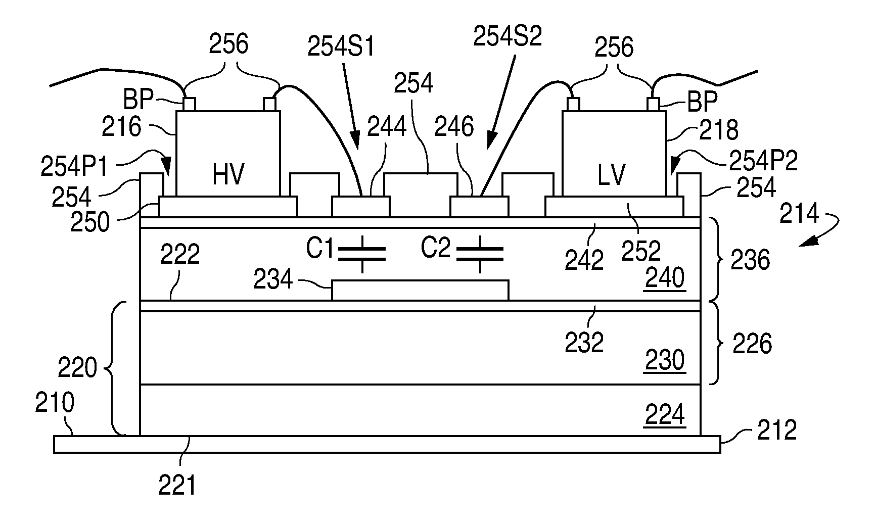
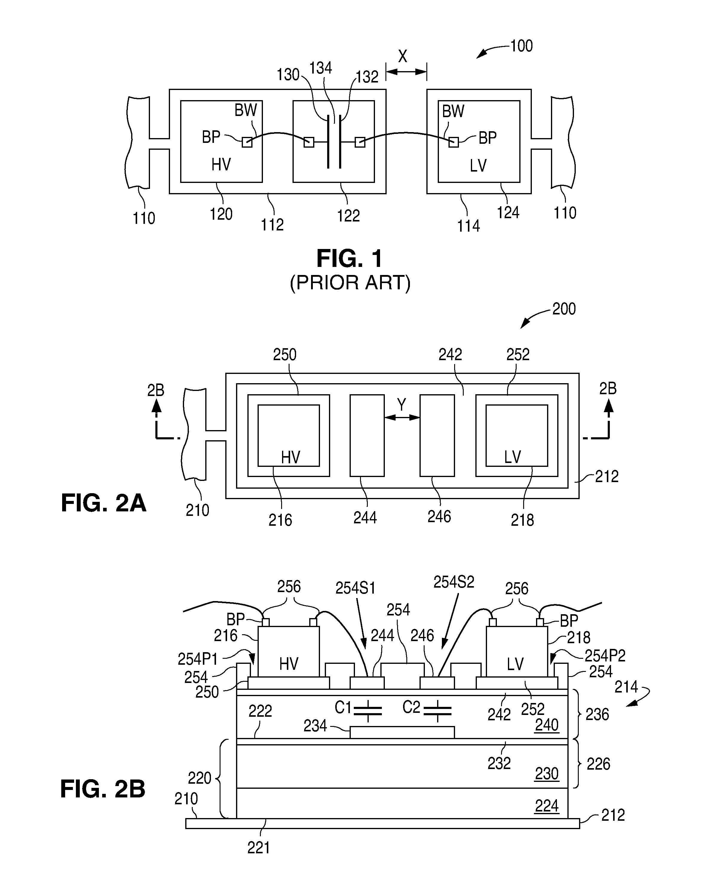
[0020]In a first embodiment, as shown in FIG. 2B, the bottom surfaces of high-voltage die 216 and low-voltage die 218 are physically connected to galvanic isolation die 214, while the bond pads BP on high-voltage die 216 and the bond pads BP on low-voltage die 218 are electrically connected to galvanic isolation die 214. High-voltage die 216 and low-voltage die 218 can both be physically connected to galvanic isolation die 214 using, for example, a conductive or non-conductive epoxy or die attach film.

second embodiment

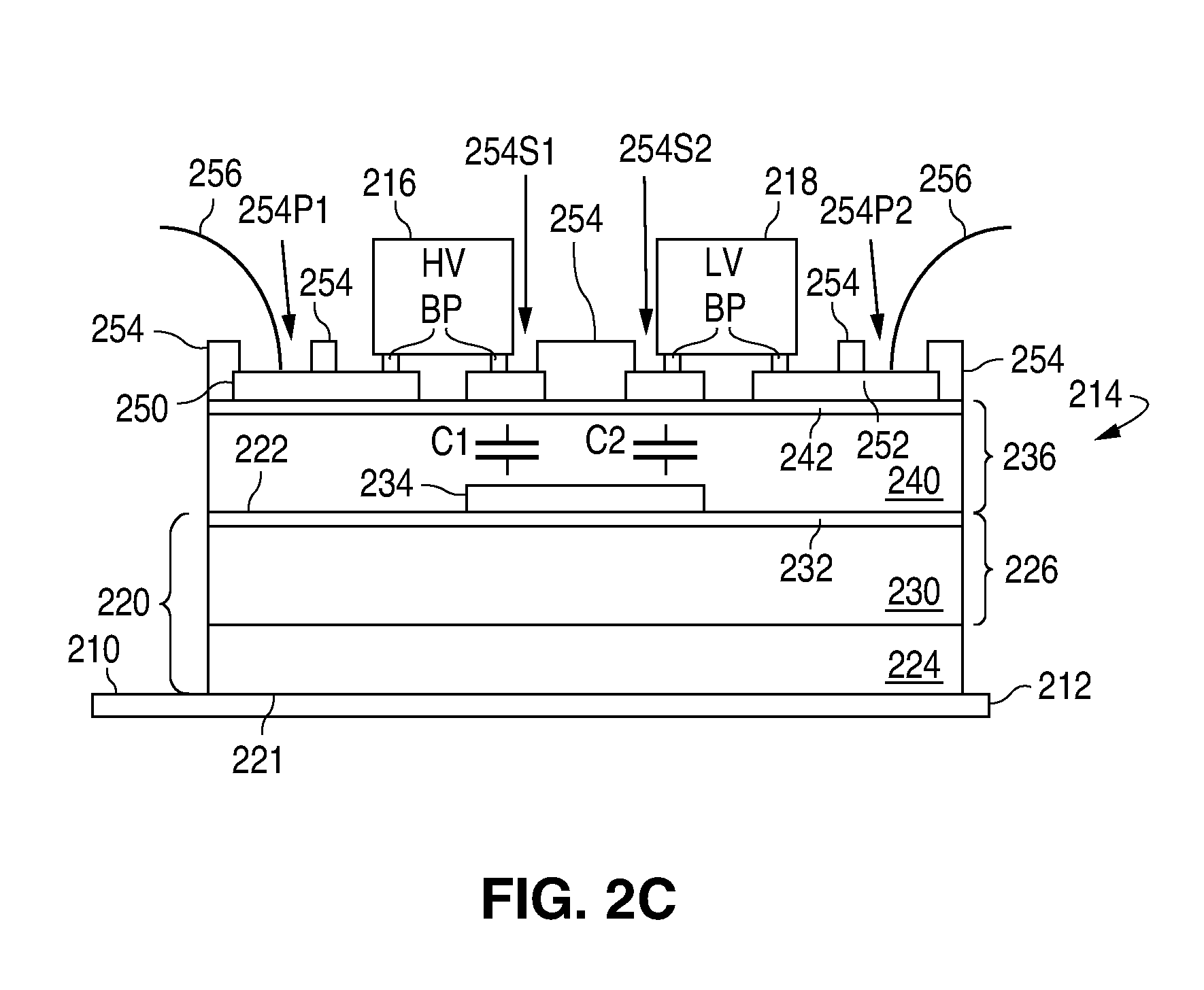
[0021]Alternately, in a second embodiment, as shown in FIG. 2C, high-voltage die 216 and low-voltage die 218 can be connected to galvanic isolation die 214 as flip chips such that the bond pads BP on high-voltage die 216 and the bond pads BP on low-voltage die 218 are electrically connected to galvanic isolation die 214. In a flip chip mounting, a conductive material, such as solder, provides both electrical and physical connection to galvanic isolation die 214. As further shown in FIGS. 2A-2C, galvanic isolation die 214 includes a substrate structure 220 which has a bottom surface 221 and a top surface 222. In the present example, top surface 222 is completely non-conductive such that no conductive structure both lies above top surface 222 and touches a conductive region that touches and lies below top surface 222.

[0022]As illustrated, substrate structure 220 can be implemented with a silicon substrate 224 and a non-conductive layer 226 that touches the top surface of silicon subst...


PUM


Abstract

Galvanic isolation between a high-voltage die and a low-voltage die in a multi-die chip is provided by a galvanic isolation die that physically supports the high-voltage die and the low-voltage die, and provides capacitive structures with high breakdown voltages that allow the high-voltage die to capacitively communicate with the low-voltage die.

Description

BACKGROUND OF THE INVENTION[0001]1. Field of the Invention[0002]The present invention relates to semiconductor structures and, more particularly, to a semiconductor structure with galvanic isolation.[0003]2. Description of the Related Art[0004]Galvanic isolation refers to an isolation that prevents a first system from communicating with a second system by way of a flow of electrons from one system to the other system, but which allows the two systems to communicate in other ways. For example, the first system can transmit a signal to the second system using changes in inductance or capacitance, or by using optical or other means.[0005]Galvanic isolation is typically implemented with a dielectric layer that lies between and electrically isolates a first conductor, such as the first coil of a transformer or the first plate of a capacitor, and a second conductor, such as the second coil of the transformer or the second plate of the capacitor. Galvanic isolation is commonly used in mult...

Claims


Application Information

Patent Timeline
Patent Type & Authority Applications(United States)
IPC IPC(8): H01L27/06H01L21/20
CPCH01L23/147H01L23/48H01L2924/30107H01L2924/10253H01L23/642H01L23/62H01L2924/19107H01L2924/15192H01L2224/73265H01L23/49531H01L23/49575H01L28/40H01L21/823481H01L21/762H01L27/0629H01L2224/16225H01L2224/32225H01L2224/48227H01L2924/00012H01L2924/00H01L24/73
Inventor FRENCH, WILLIAMHOPPER, PETER J.GABRYS, ANN
Owner NAT SEMICON CORP
Why Eureka
Try Eureka