Semiconductor device and method for fabricating the device

Active Publication Date: 2013-02-21
PANASONIC CORP
View PDF2 Cites 29 Cited by
  • Summary
  • Abstract
  • Description
  • Claims
  • Application Information

AI Technical Summary

Benefits of technology

[0031]According to the semiconductor device disclosed in this description, a gap is selectively left at the bottom of a trench that is arranged in a semiconductor layer, thereby defining an insulating region, which is thicker at the bottom of the trench than on the side surface of the trench, between the conductive layer to be a gate electrode and the semiconductor layer inside of the trench. In addition, by setting the thickness of the insulating region at the bottom of the trench to be greater around the center of the trench than beside the side surface of the trench, it is possible to prevent the electric field from going excessivel

Problems solved by technology

In a MISFET with the trench gate structure, however, the intensity of the electric field applied to the gate insulating film 6 becomes very high, which is a problem.
That is why in almost all cases, breakdown will occur in the

Method used


Image

  • Semiconductor device and method for fabricating the device
  • Semiconductor device and method for fabricating the device
  • Semiconductor device and method for fabricating the device

Examples


embodiment 1

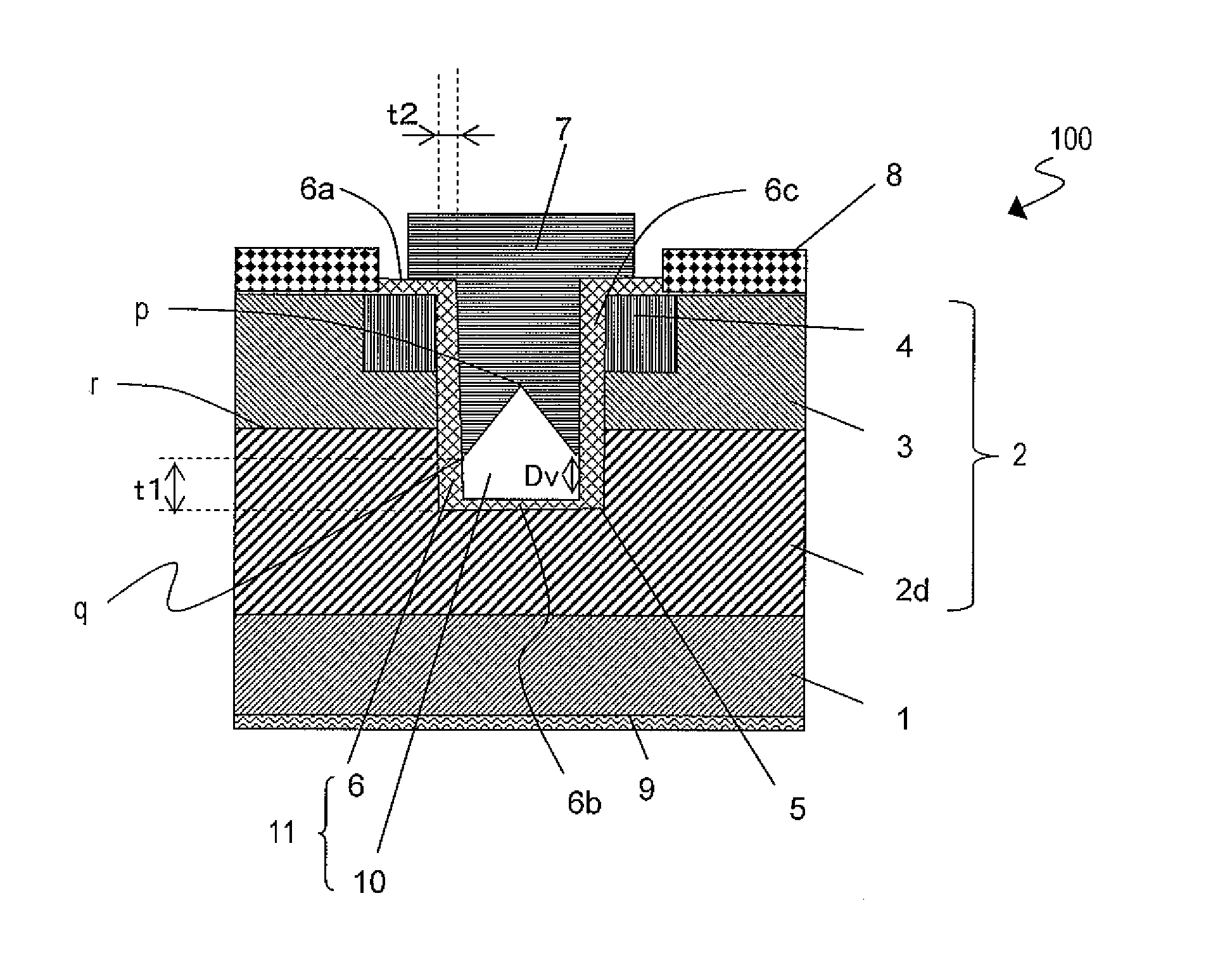
[0053]Hereinafter, a first embodiment of a semiconductor device according to the present invention will be described with reference to the accompanying drawings. The semiconductor device of the first embodiment is a silicon carbide MISFET with a trench gate structure. However, this embodiment does not have to be applied to such a silicon carbide MISFET but may also be applicable to any other silicon carbide semiconductor device such as a silicon carbide MESFET or a semiconductor device that uses any other wide bandgap semiconductor (such as GaN, AlN or diamond) instead of silicon carbide.

[0054]The semiconductor device of this embodiment includes a plurality of unit cells that are arranged two-dimensionally. FIG. 1(a) is a cross-sectional view illustrating a part of the semiconductor device 100 and FIG. 1(b) is a plan view illustrating an exemplary arrangement of a unit cell 100U on the surface of the silicon carbide layer of the semiconductor device 100. FIG. 1(a) is a cross-section...


PUM


Abstract

The semiconductor device 100 of this invention includes: a semiconductor layer 2 arranged on the principal surface of a substrate 1 and made of a wide bandgap semiconductor; a trench 5 which is arranged in the semiconductor layer 2 and which has a bottom and a side surface; an insulating region 11 arranged on the bottom and side surface of the trench 5; and a conductive layer 7 arranged in the trench 5 and insulated from the semiconductor layer 2 by the insulating region 11. The insulating region 11 includes a gate insulating film 6 arranged on the bottom and the side surface of the trench 5 and a gap 10 arranged between the gate insulating film 6 and the conductive layer 7 at the bottom of the trench 5. The gate insulating film 6 contacts with the conductive layer 7 on a portion of the side surface of the trench 5 but does not contact with the conductive layer 7 at the bottom of the trench 5. The thickness of the insulating region 11 measured from the bottom of the trench 5 through the lower surface of the conductive layer 7 is greater around the center of the trench than beside its side surface.

Description

TECHNICAL FIELD[0001]The present invention relates to a semiconductor device that uses a wide bandgap semiconductor, and more particularly relates to an MIS semiconductor device with a trench gate structure and a method for fabricating such a device.BACKGROUND ART[0002]Wide bandgap semiconductors have been used extensively in various kinds of semiconductor devices including power elements (which will also be referred to herein as “power devices”), hostile-environment elements, high temperature operating elements, and radio frequency elements. In particular, application of such a material to power devices such as switching elements and rectifier elements has attracted a lot of attention.[0003]Among those wide bandgap semiconductors, power devices that use silicon carbide (SiC) (which are also called “SiC power devices”) have been developed particularly extensively because a SiC substrate can be made relatively easily and because silicon dioxide (SiO2) can be obtained as a gate insula...

Claims


Application Information

Patent Timeline
IPC IPC(8): H01L29/24H01L21/336
CPCH01L21/044H01L29/2003H01L21/28264H01L29/42368H01L29/42376H01L29/4238H01L29/515H01L29/66045H01L29/66068H01L29/66734H01L29/7397H01L29/7813H01L29/7828H01L29/1602H01L29/1608H01L21/049
Inventor SORADA, HARUYUKI
Owner PANASONIC CORP
Why Eureka
Try Eureka